
Products
Fluxes
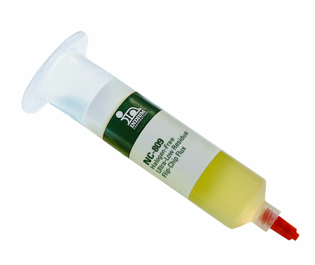
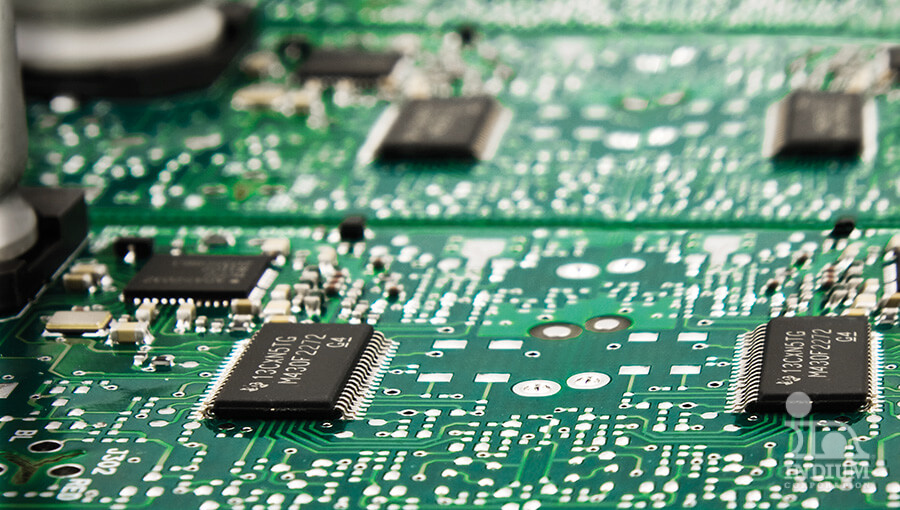
Indium Corporation manufactures a variety of high-quality, proven flux products, ranging from wave flux to semiconductor fluxes, such as true no-clean flip-chip flux, which we first introduced in various applications, including the most advanced 2.5D chip on wafer package application. Our flux products are formulated for superior performance to serve virtually any application where flux is required.
Powered by Indium Corporation
- Wide Portfolio
- True No-Clean
- Excellent Tech Support

Product Overview
As pioneers in the semiconductor industry, we lead the market in no-clean flux solutions. We introduced the first true no-clean flip-chip flux, now widely adopted by major OSATs. Our innovative formulas support the evolution of packaging technology, enabling smaller, thinner, and more powerful designs for the next generation of development.
Features
First No-Clean
We introduced the first true no-clean flip-chip flux and continue to innovate more ultra-low residue flux formulas.
True One-Step
We provide true water-wash flux such as WS-446HF, demonstrating outstanding performance on Cu-OSP, streamlining the process by eliminating extra cleaning steps that typically involve additional flux to remove excessive oxides.
Proven
Our fluxes are widely adopted by leading EMS, OSATs, and OEMs in various applications.
Flux Products
Our extensive selection of flux products includes PCBA and semiconductor fluxes, catering to diverse applications across multiple industries.
PCB Assembly Fluxes
PCBA Fluxes include wave, rework, and package-on-package…
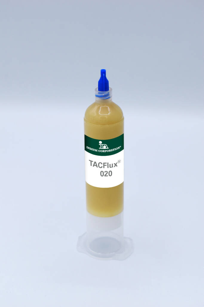
Semiconductor Fluxes
Extensive portfolio of proven and new semiconductor…

Ball-Attach Flux
High-quality water-wash and no-clean ball-attach fluxes.
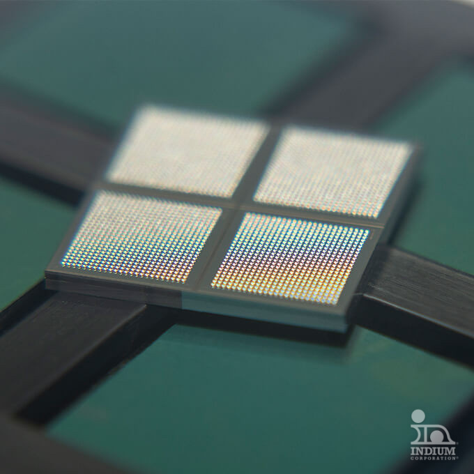
Flip-Chip Flux
Offers advanced fluxes for flip chip assembly,…
Rework Flux
PCBA rework fluxes for efficient rework, repair,…
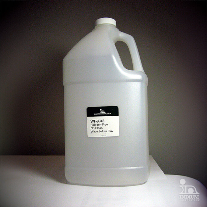
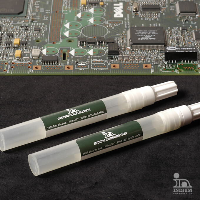
Wave Flux
Meet the highest standards with cutting-edge wave…
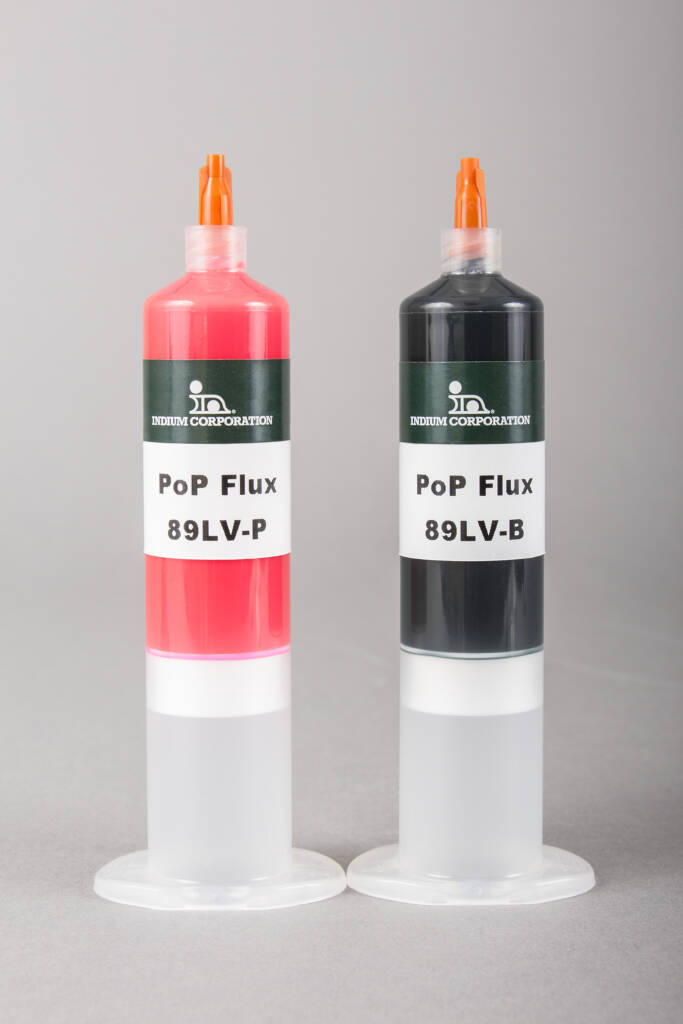
Package-on-Package Flux
Package-on-Package flux for high yields and optimal…
Wafer Bumping Flux
High-quality wafer bumping fluxes for efficient removal…

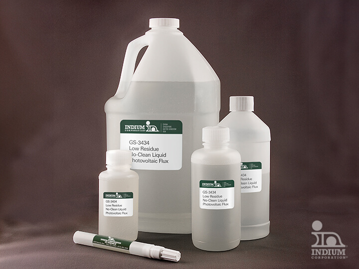
Solar Tabbing Fluxes
Solar Tabbing Fluxes are designed for photovoltaic…
Related Applications
Indium Corporation’s Flux products cover a wide-range of applications.
PCB Assembly
Proven and cutting-edge materials for PCB assembly…

Semiconductor Packaging and Assembly
Critical semiconductor packaging ensures functionality and durability.

Power Electronics Packaging & Assembly
Extensive range of proven high-reliability solder and…
Related Markets
Flux products are suitable for many markets across multiple industries.


Expert Support for Reliable Results
Do you have technical questions or sales inquiries? Our dedicated team is here to help. “From One Engineer to Another®” isn’t just our motto—it’s our commitment to delivering exceptional service. We’re ready when you are. Let’s connect!

Looking for Safety Data Sheets?
Access everything you need — from technical specifications to application guidance — in one convenient location.

Your Success
is Our Goal
Optimize your processes with the latest materials, technology, and expert application support. It all starts by connecting with our team.