SMT Optimization for Success
Part 6: Solder Paste Particle Size and Its Effect on Stencil Printing Ultra-fine Solder Paste Deposits
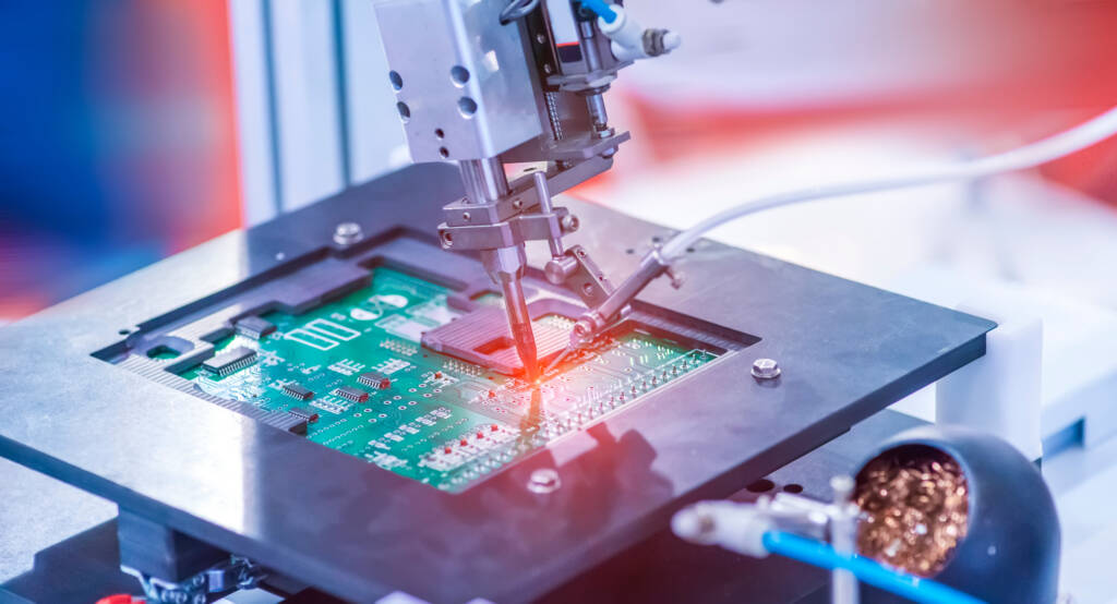
This final post in a series on the stencil printing aspect of SMT optimization using ultrafine solder paste pulls together everything we have discussed previously as we look at the effect of solder particle size. I presented some of the following information at the Toronto SMTAI in May 2014. These findings are based on a solder paste printing experiment designed to differentiate the transfer efficiency and consistency between different solder powder types. In an effort to diminish the number of variables, the same stencil, squeegee blades, and printer parameters were utilized.
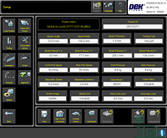
Figure 1. Experiment printer settings
A 4 mil-thick laser-cut stencil, 250 mm squeegee with edge guards, foilless clamps, and landscape vacuum support blocks were used. Figure 1 depicts the printer settings utilized for the experiment. Each solder paste was printed at 50mm/s with a blade pressure of 4.4kg, 5mm/s separation speed, and a separation distance of 2mm. The underside stencil-wipe method was used only during the 1-hour pause wet/dry/vacuum (W/D/V).
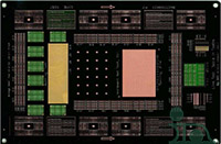
Figure 2. Test vehicle
A test vehicle (Figure 2) was selected with focus on 6, 7, 8, 9, 10, & 12mil circles and squares, as well as 0201 pads in both solder mask-defined (SMD) and non-solder mask-defined (NSMD) pads. Four powder types were evaluated (3, 4, 5, and 6) in no-clean and water soluble flux formulations. Response-to-pause was measured by continuously printing 20 times, pausing for 1 hour, then printing 6 more times. A W/D/V stencil wipe was incorporated immediately after printing the first 20 PWBs. A Koh Young KY-3020T laser scanning system was used to measure the volume of the stencil printed deposits. 1,386,500 data points (solder paste deposits) were collected.
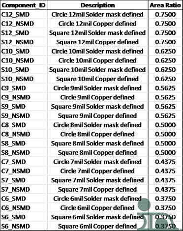
Figure 3. Pad labels, description, and associated area ratios
Figure 3 shows the component identification and the area ratio associated with it.
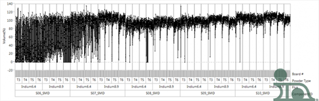
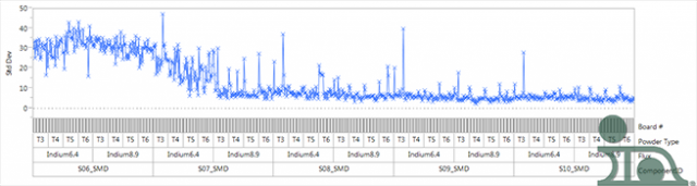
Figure 4. A broad view of test results
Figure 4 represents a broad view of the resultant test data. The y-axis of the upper graph indicates the transfer efficiency in volume %. The bottom graph indicates the standard deviation of the process: <10% standard deviation and 100% transfer efficiency is our goal.
In our investigative process we eliminated test data for 0201 and 12mil chip-scale package (CSP) test pads: these are not depicted in Figure 4. The solder paste deposits on these pads were well-printed regardless of powder and flux type and were, therefore, excluded from further investigation. The data in Figure 4 reveals that the smallest test aperture (6mil) did not print well for all powder types or flux vehicles. The area ratio is quite small (0.375) for the 6mil aperture and the results were inconsistent, to say the least.
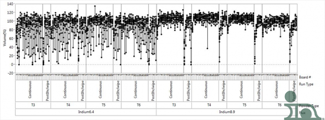
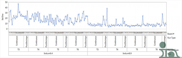
Figure 5. Example results of 7mil square solder mask defined pad
Figure 4 revealed a dramatic improvement with 7mil apertures that deserved further investigation, notably between the water-soluble and no-clean flux formulations. Figure 5 shows the improvement in more detail by expanding the view of the 7mil aperture and breaking out the data before and after the 1-hour pause. The comparison is very typical when comparing no-clean and water-soluble solder pastes. Note that a standard deviation of <10%, with the exception of a few outliers was evidenced, specifically with the no-clean flux chemistry (Indium8.9). The area ratio for the 7mil aperture is 0.4375. The transfer efficiency was near the target (100%) and improved as the powder type moved toward type 6. Type 5 exhibited the best results—a narrow distribution in volume percent and low standard deviation except after first pause. It is important to note that the significant drop in transfer efficiency after the 1-hour pause was not consistent with previous experiments. For all solder pastes tested, this was attributed to a very low humidity (<10%) and had a dramatic effect on the first print after sitting on the stencil for 1 hour.
The best area ratio achieved in the experiment was 0.4375 using all the optimization processes/guidelines covered in the previous posts. The finer powder, in conjunction with solder mask defined pads, square aperture with radius corner stencil apertures, and no-clean flux chemistry, achieved an improved area ratio.