Part 5: Solder Mask Defined vs. Copper Defined (Non-Solder Mask Defined) Pads
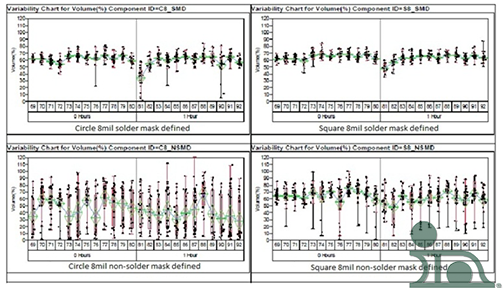
Figure 1.
In the last discussion we statistically evaluated and concluded that square apertures with radius corners provided more consistent (less standard deviation) paste deposits than circular apertures of the same area ratio (8mil circle and square, 4mil thick stencil both equate to an area ratio of 0.50). Figure 1 reveals that we can improve our results by changing the location of the solder mask in relation to the PCB pad-by using either solder-mask-defined or non-solder-mask-defined (sometimes referred to as copper-defined) pads.
The boxplot diagrams depict transfer efficiency in volume percent on the y-axis; shown are four separate charts representing 8mil circles and squares. Note the bottom two graphs show erratic and inconsistent paste release for the non-solder-mask-defined or copper-defined pads for both circles and squares. The top boxplot diagrams illustrate a dramatic improvement (much tighter distribution, far less outliers) for both circles and squares with solder-mask-defined pads. The best results were shown with the square (radius corners), solder-mask-defined, providing a very tight distribution and no outliers.
These results have been confirmed in several trials, both internally and with customers. Note that our discussion is focused on optimization for ultrafine stencil printing; for larger apertures, (>12mil) there may little or no difference.
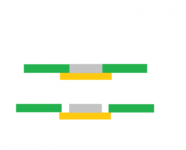
Figure 2.
Why, you may ask?
Figure 2 illustrates a paste deposit on mask-defined (top) and copper-defined (bottom) pads. Paste release from the stencil aperture is aided by the adhesion of the solder paste to the PWB pad. The adhesion helps to pull the solder paste from the stencil aperture as the PWB is lowered from the stencil. There is very little surface area for this adhesion to occur with smaller apertures. The walls of the solder mask itself add to the total surface area for the solder paste to adhere to. The increased surface area aids in pulling the solder paste from the stencil aperture. Stencil aperture reductions would obviously negate this affect, but, because the area ratio is already very low (0.50 for 8mil aperture, 4mil thick stencil), most often the smaller apertures are printed one-to-one, or even a little larger.
We are near the end of our series on process optimization; the next segment on stencil printing looks at particle size. The last segment will cover reflow profiling.