
Thông lượng bán dẫn
Thông lượng va chạm wafer
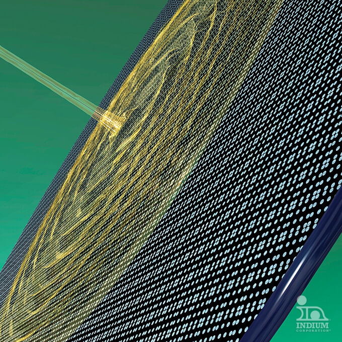
Indium Corporation creates and provides top-tier wafer bumping (bump fusion) fluxes designed to eliminate oxides and other contaminants during reflow and cleaning. Our fluxes can be applied to solder-bumped and copper-pillar/solder-capped wafers through dispensing or spin coating techniques.
Được cung cấp bởi Indium Corporation
- Water-Washable or Solvent-Cleanable
- Suitable for Use with Various Alloys
- Tương thích rộng rãi
Tổng quan sản phẩm
Indium Corporation boasts a longstanding reputation for delivering high-quality wafer-bumping fluxes. Our extensive portfolio features materials tailored for various applications, including traditional wafer bumping processes where fluxes are spin-coated onto plated bumps or copper pillars. Additionally, our products excel in printing applications, where flux is applied to wafers before a ball drop process, commonly used in wafer-level CSP (WLCSP), as well as wafer-level and panel-level fan-out packages.
Our wafer-bumping flux products are compatible with polymers and passivation materials commonly used in wafer processing and packaging assembly.
- Applied by jetting or dispense, followed by spin coating to optimize film thickness
- Reflow in inert atmosphere (typically <20ppm O2 level)
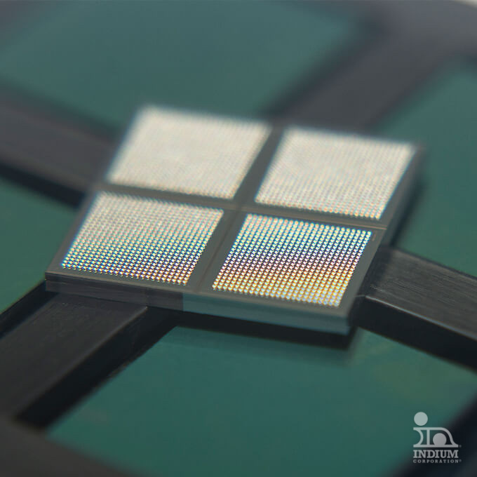
- Converts rough, non-spherical, plated, or wafer probe-dented solder bumps into shiny oxide-free bumps
- Proven applications include copper-pillar microbumps and standard solder bumps
- Applied by printing onto wafer or panel using screen or stencil, followed by a ball drop process
- Wafer bumping flux WS-3401 is used in most advanced 2.5D chip on wafer packaging technology.
- Wafer bumping flux SC-5R has been used for over 10 years in legacy products.
Wafer Bumping Flux Products
Wafer bumping with flux continues to be a widely used method, although some have transitioned to flux-less equipment and processes. Flux is highly effective in producing uniformly low-oxide and well-rounded bumps with optimal morphology.
| Flux Type* | Phương pháp ứng dụng Flux | Sự miêu tả | Phương pháp vệ sinh | Không có Halogen | Vật liệu |
|---|---|---|---|---|---|
| SC | Dispence/Spin Coating | High-Pb, SnPb-eutectic, and SnAg solder bumps | Solvent- or aqueous-based chemistry | Đúng | SC-5R |
| WS | Dispence/Spin Coating | 20-65 micron pitch copper-pillars with SnAg or Sn100 microbumps | Nước DI ấm | Đúng | WS-3401 WS-3543 |
| Flux Type* | Phương pháp ứng dụng Flux | Sự miêu tả | Phương pháp vệ sinh | Không có Halogen | Vật liệu |
|---|---|---|---|---|---|
| WS | In ấn | 0.5mm and smaller pitch wafer-level or panel-level package; also suitable for LED die-attach application | Nước DI ấm | Đúng | WS-676 WS-759 WS-829 |
| Considerations | Solder Paste Printing | Plating | Flux/Solder Ball Printing | C4-NP (Suess/IBM) |
|---|---|---|---|---|
| Used In High Volume Manufacturing? | Đúng | Đúng | Đúng | Đúng |
| Alloy Restrictions | All solder alloys, as long as powder can be made | Binary alloys only (Sn/Pb, Sn/Ag, Sn/Cu etc.) due to alloy control issues | All solder alloys, as long as sphere can be made | Probably limited to binary alloys |
| Bump Size | Down to around 125micron pitch only. Only 45% of paste volume is metal | Down to 2micron bumps feasible: possibly less | 60micron bump diameter in mass production, but most commonly used for wafer level CSP manufacturing | Unknown |
| Bump Uniformity | OK: can vary significantly with age of solder paste and print process variables | Good | Good with appropriate tight tolerance solderspheres | Good |
| Làm mất hiệu lực | Common | Little or no with a controlled plating process | Little or no | Little or no |
| Cost Comparison | Low Cost | More Expensive | Low Cost | High Capital Cost |
| Prototyping | Fairly Easy | Complex | Easy | Complex |
Bảng dữ liệu sản phẩm
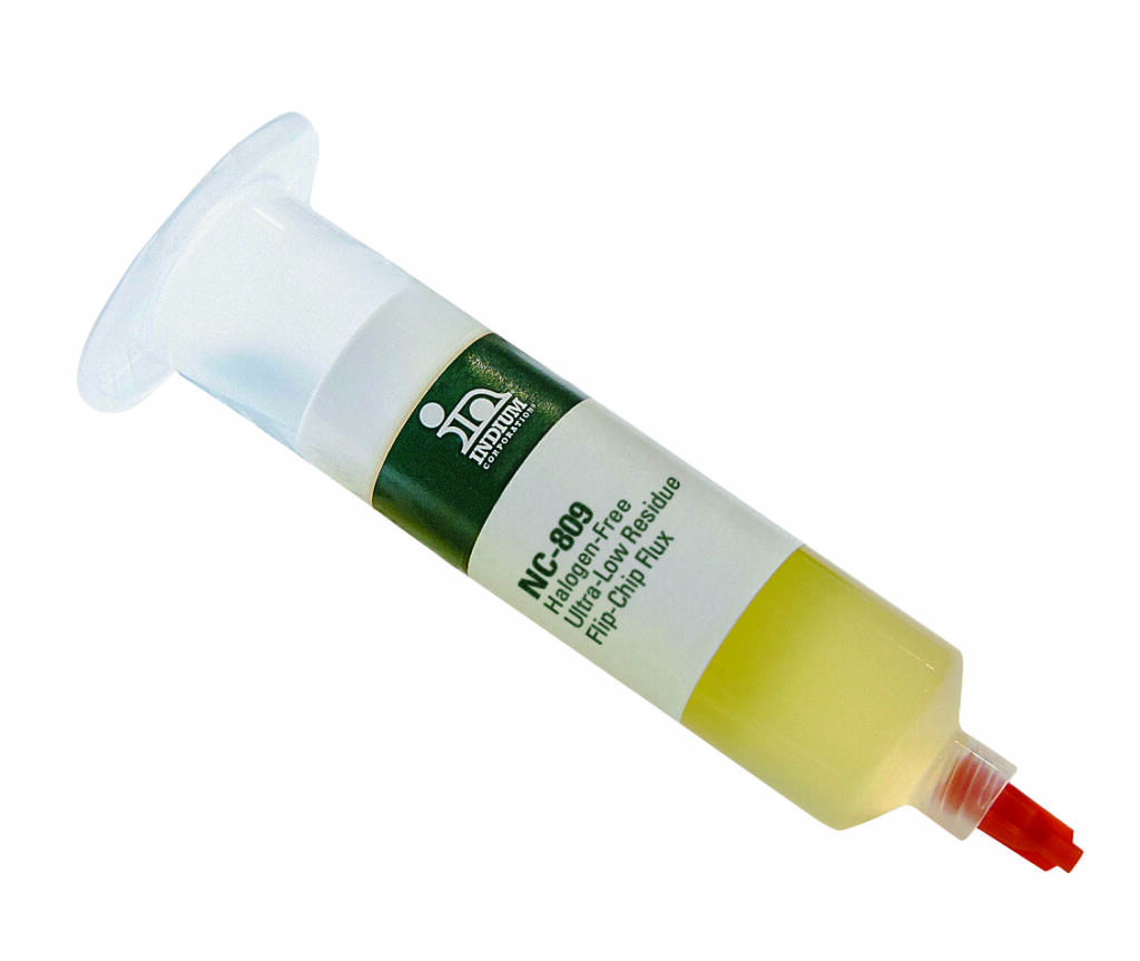
WS-3401 Chất trợ dung wafer PDS 98197 R4.pdf
WS-3401-A Chất trợ dung wafer PDS 98764 R4.pdf
WS-3518 Wafer Flux PDS 98431 R3.pdf
WS-3543 Chất trợ dung wafer PDS 98398 R3.pdf
Ứng dụng liên quan

Đóng gói và lắp ráp chất bán dẫn
Bao bì bán dẫn quan trọng đảm bảo chức năng và độ bền.
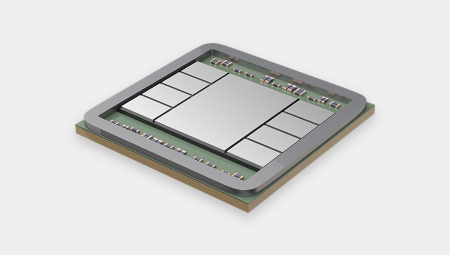
Bao bì 2.5D và 3D
Techniques to incorporate multiple dies in a…
Flip-Chip
A crucial technique in advanced semiconductor packaging.
Thị trường liên quan


Sản phẩm liên quan
Thông lượng bán dẫn
Extensive portfolio of proven and new semiconductor…

Thuốc thông gắn bi
High-quality water-wash and no-clean ball-attach fluxes.
Thông lượng Flip-Chip
Offers advanced fluxes for flip chip assembly,…
Hỗ trợ chuyên gia cho kết quả đáng tin cậy
Bạn có thắc mắc về kỹ thuật hoặc yêu cầu bán hàng không? Đội ngũ tận tâm của chúng tôi luôn sẵn sàng trợ giúp. “Từ kỹ sư này đến kỹ sư khác®” không chỉ là phương châm của chúng tôi—mà còn là cam kết của chúng tôi trong việc cung cấp dịch vụ đặc biệt. Chúng tôi luôn sẵn sàng khi bạn sẵn sàng. Hãy kết nối!

Bạn đang tìm kiếm Bảng dữ liệu an toàn?
Truy cập mọi thứ bạn cần — từ thông số kỹ thuật đến hướng dẫn ứng dụng — tại một vị trí thuận tiện.

Sự thành công của bạn
là Mục tiêu của chúng tôi
Tối ưu hóa quy trình của bạn với vật liệu, công nghệ mới nhất và hỗ trợ ứng dụng chuyên gia. Tất cả bắt đầu bằng cách kết nối với nhóm của chúng tôi.