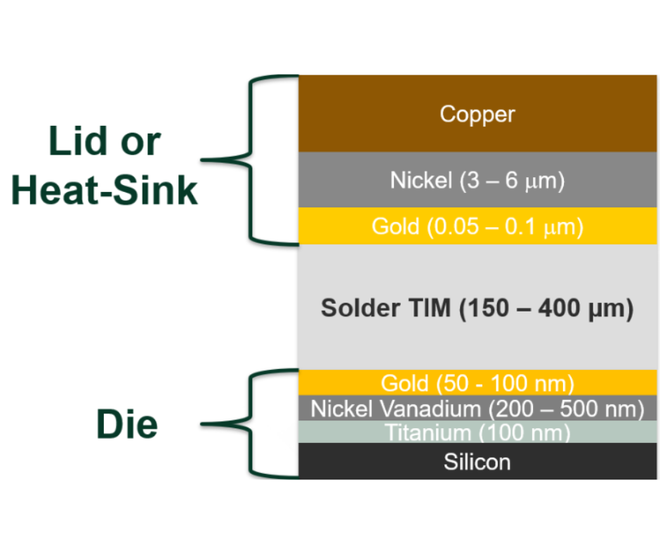
Solderability and Wetting
The wetting and spreading of solder onto surfaces is an essential part of forming a strong, reliable, conductive joint. The term "solderability"is a way of talking about how quickly and evenlythe solder spreads onto a surface, with strong, low-voiding solder joints always resulting from good wetting. It's also a very loose term as it combines elements from both kinetics and thermodynamics. The main driving force for good solderability is thermodynamic:the negativefree energy of formation of an intermetallic formed when liquid solder contacts a solid metal surface, favoring the contact of the liquid metal with the metal surface.
It's that simple.
Solderability Preserving Coatings
There are other factors that complicate things, such as protective coatings. These are in two forms:
– Evanescent organic materials, such as OSPs (organic solderability protectants) that are most commonly chemisorbedonto surfaces (usually copper) to slow the rate ofoxidation of the underlying metal, yetare designed to be easily removed during the reflow process by a combination of volatilization and solubilisation in flux.
– Sacrificial metal layers (SML) that dissolve quickly into the liquid solder after completing their task of protecting the underlying metal surface against oxidation. Examples are Ag/Ni and ENIG (Au/Ni): in each case, thenickel is kept oxide-free by the protective solder-soluble metal. Too thin a SML and pinholes in the SML will allow the nickel to oxidize: too thick a layer andSML/solder intermetallics may form,and interfere with both the SML solubility and the solder's wetting speed.
Voiding
We know that goodsolderability (with its corollary:low voiding), is critical to power device manufacturers, with die-attach voiding criteria commonly set for discrete devices at 5% (single void) <10% (total), while IGBT voiding restrictions may go from <2% all the way down to <0.5%. In each case, the %voiding is an area percentage of the total solder joint area.
Nitrogen (low ppm oxygen) reflow is critical for high temperature soldering, of course, with the usage of forming gas (H2/N2) sometimes giving benefits for some surfaces such as nickel and copper. For very low voiding with large area die (10x10mm and higher), vacuum reflow is usually essential.
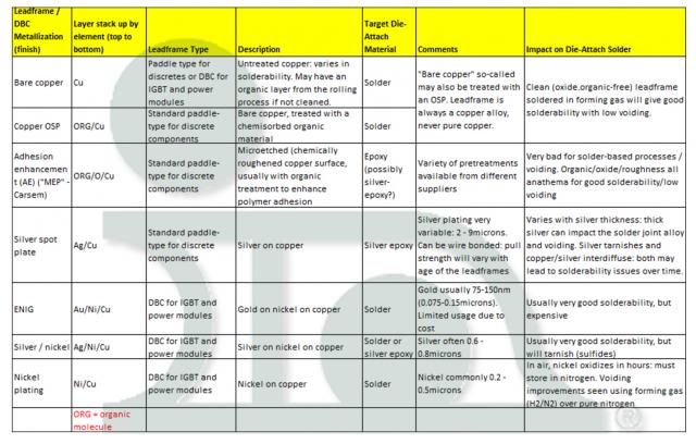
Choosing a Leadframe
We have recently been working with several customers on both standard leaded (Pb-containing) solder pastes, and our new HT Pb-free solder paste technology, the BiAgX(®), with changes of leadframe surface being made necessary. In this case, customers are moving from precious metal plating on copper, to "bare" copper, resulting in some cost savings as well as enabling a transition to a Pb-free die-attach solder.
Below is a guide for power semiconductor users in choosing an appropriate leadframe or DBC finish.
Many thanks to my colleagues Karthik Vijayamadhavan (Europe), Sehar Samiappan and SzePei Lim (South East Asia), David Hu (Hu Di) (China) and Dr Hongwen Zhang (USA) for their comments and input.