Library
Blog
Topic
Type
Year
Author
Product Type

Good Solder Paste Response-to-Pause Increases Profability Part 2
Folks, Let’s check in on Megyn Woodley as she helps Andover Electronics solve their response-to-pause problem… Megyn Woodley had performed response-to-pause experiments on the solder paste that
Good Solder Paste Response-to-Pause Increases Profitability Part 1
Megyn Woodly had just finished a three-day audit of Andover Electronics Assembly’s four assembly lines. She felt the factory was well organized, run with high first-pass yields, and quite good
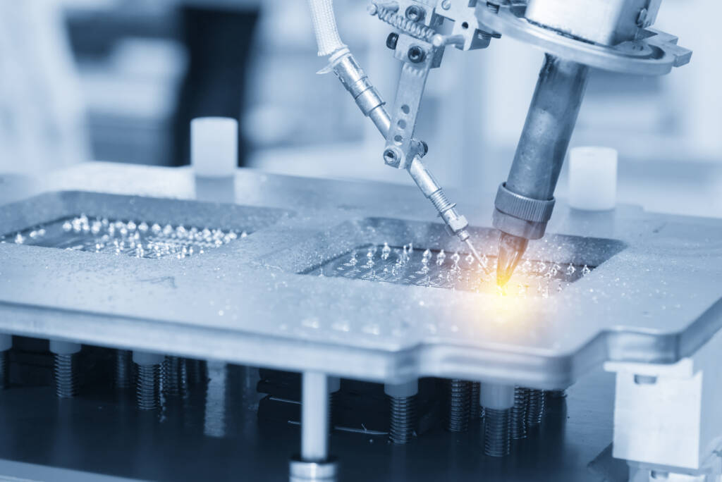
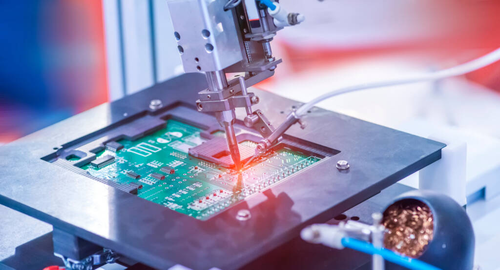
Robotic Soldering, Smarter (Part 3): Indium Corporation’s Innovation and the Future of Robotic Soldering
In Part 2, we outlined materials challenges that can impact robotic soldering performance. In Part 3, we shift to product solutions and emerging innovations—highlighting how cored wire performance
Robotic Soldering, Smarter (Part 2): Tackling Common Materials Challenges in Robotic Soldering
In Part 1, we covered how robotic soldering evolved, and why materials quality is a major driver of process stability and precision. In Part 2, we focus on common materials-related issues that can

Robotic Soldering, Smarter (Part 1): From Automation to Materials That Make It Reliable
Robotic soldering has evolved from a productivity upgrade into a precision requirement—especially as electronics become smaller, denser, and require shorter production cycles. In Part 1 of this
The Electron: A Biography and the Rise of Modern Electronics
Folks, In my last post, we explored the dawn of electricity and the early days of radio. Now, we move further along the history of electronics timeline to see how everyday consumer products forced
The Electron: A Biography and the Emergence of Soldering
Folks, My interest in the history of electronics was piqued when I attended a mid-1990s lecture by Noble Laureate Arno Penzias on the same topic. Penzias was a co-discover of the Cosmic Microwave
Rethinking Your Alloy Strategy: How to Win with Low-Silver Solder
Silver prices are escalating rapidly, consistently trending upward. If you manage a bill of materials (BOM) for electronics manufacturing, you understand precisely how this volatility impacts your

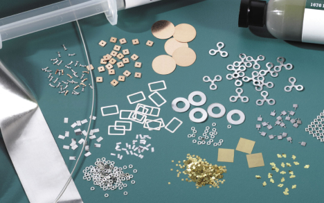
Mastering Assembly Consistency with InFORMS® Solder Preforms
Manufacturing modern electronics often feels like a balancing act—literally. Assembly tilt and uneven coplanarity are persistent headaches that compromise solder joints, leading to weak connections

The Crystal That Solves AI’s Data Bottleneck – GGG
This is not a diamond. Can you believe this crystal contains gallium? Yes, this is a garnet crystal of gadolinium gallium, commonly called GGG, with the chemical formula Gd3Ga5O12. GGG crystals are
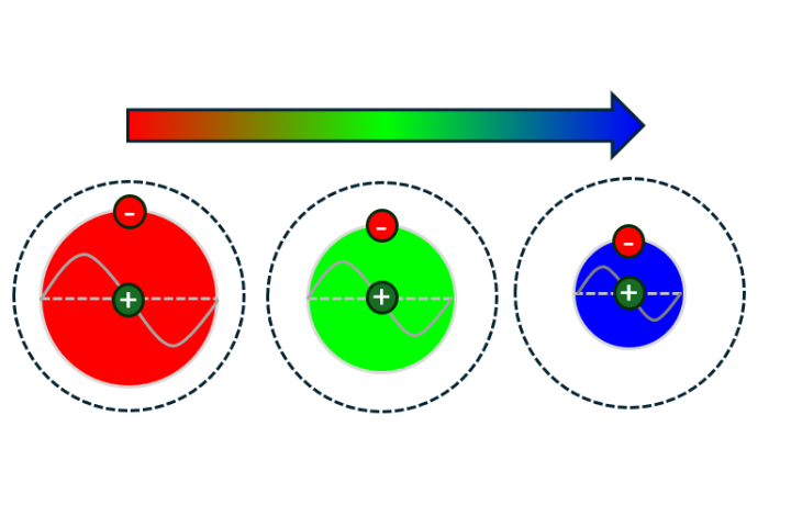
The Physics Behind Quantum Dots
The discussion below leans into technical language and uses terms commonly established in quantum mechanics and semiconductor physics. Quantum dots are one of the clearest real-world examples of
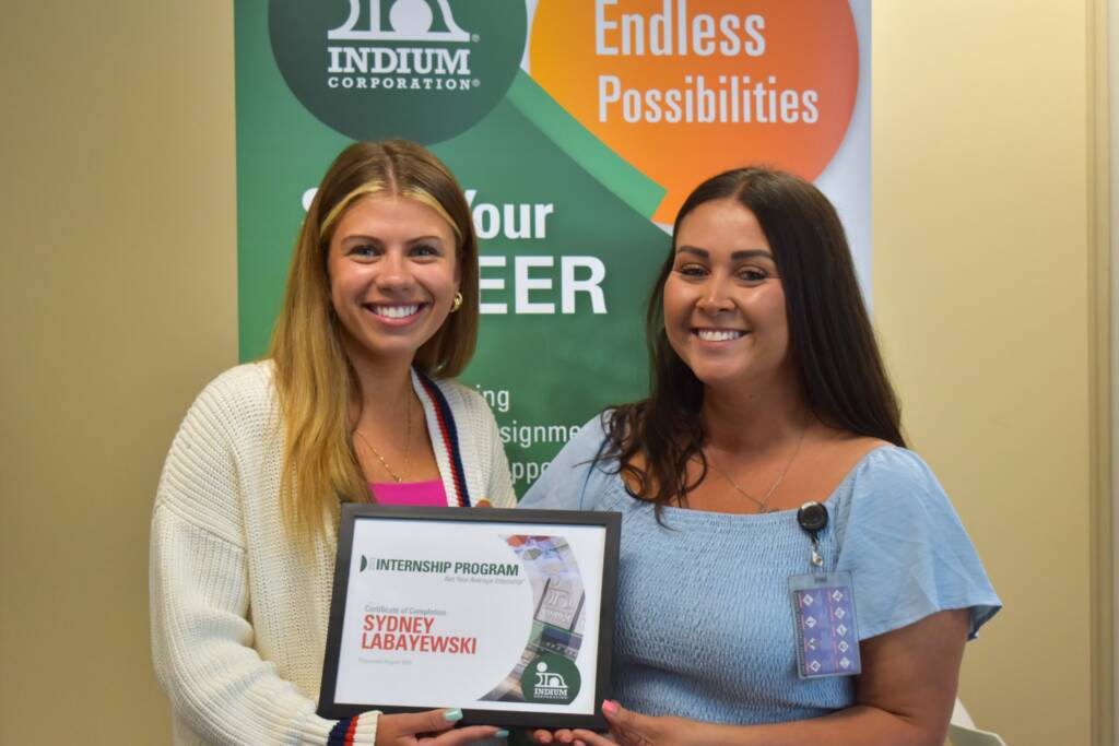
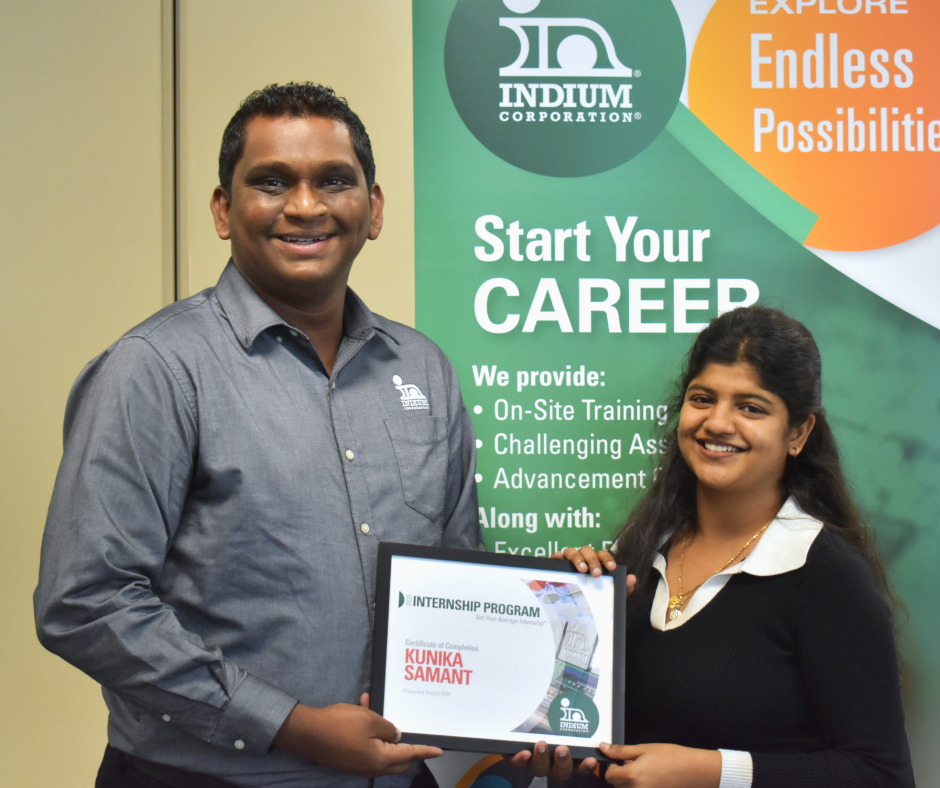
Understanding the Puzzle: A Summer in Marketing Communications
Looking back on my internship with Indium Corporation, one of the most significant lessons I’m taking with me is the importance of understanding how all the pieces of a team fit together. Long-term

Hypothesis Test for Two Samples
Professor Patty Coleman was in her office at Ivy University contemplating a truism. Both she and her husband Rob worked at Ivy U, but they couldn’t afford to send their twin sons

Excel® Software Tool to Perform Hypothesis Tests on SMT Data
Ivy University Professor Patty Coleman was at Simon Pearce Restaurant, having a solo lunch and relaxing as she watched the beautiful waterfall at the restaurant. As she enjoyed their signature

My Experience Living in a Different Country
Stepping Outside My Comfort Zone Traveling more than 3,000 miles to live and work in another country is the most daunting thing I’ve ever done. Luckily, I came to work for Indium Corporation.

Pressure, Process, and Progress: An Intern’s Guide to Debugging the Workplace
Starting a professional internship is always nerve-wracking. I still remember the nervousness I felt heading into orientation day. I spent my overnight flight across the country to Utica wondering
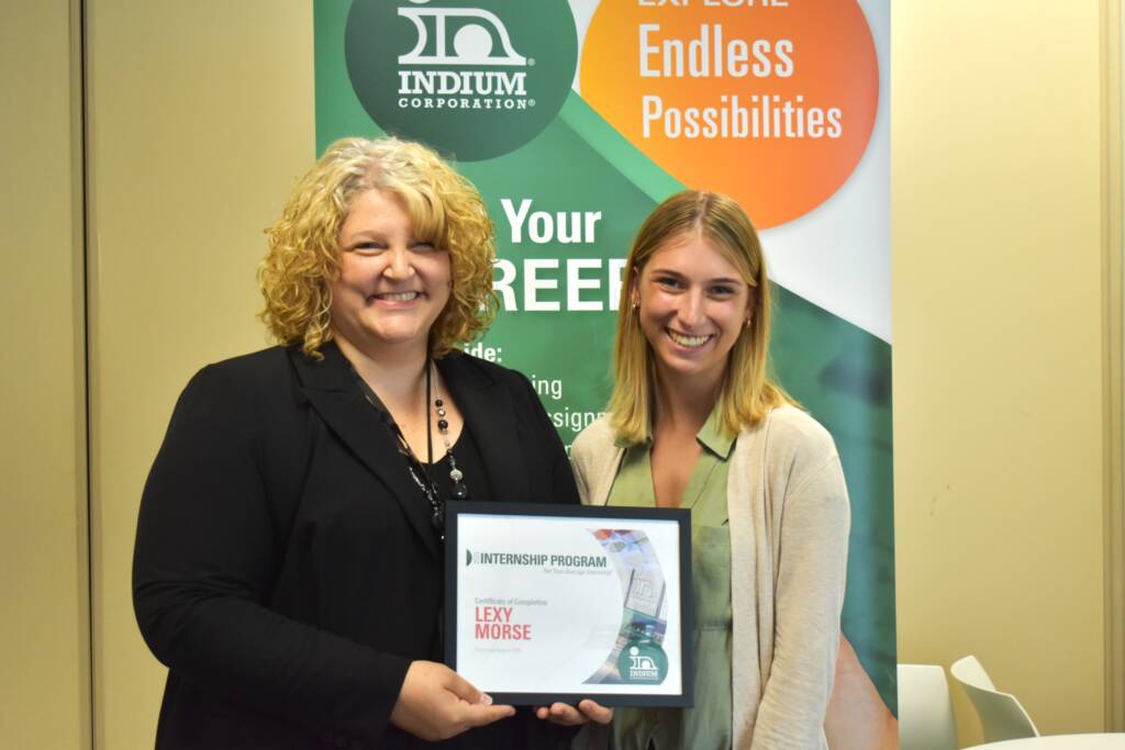
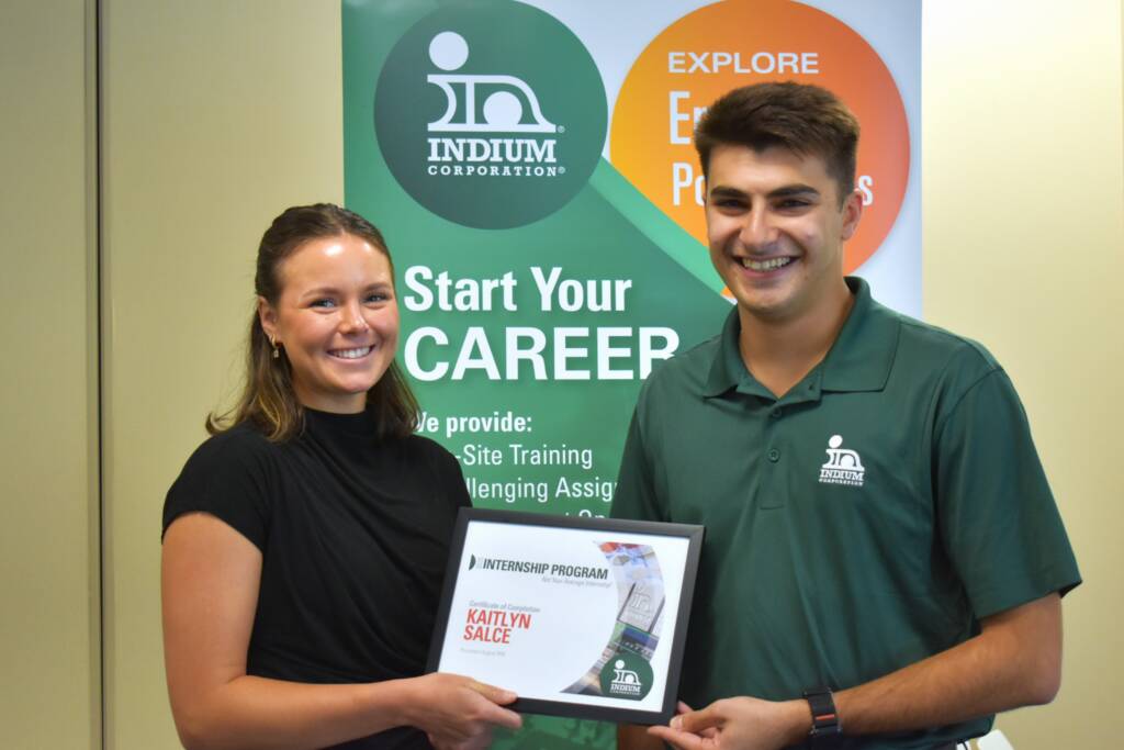
Why I Came Back to Indium Corporation as an Operational Excellence Intern
Starting My Journey at Indium Corporation In the summer of 2024, I was looking for work and unsure where my next opportunity would come from. Fortunately, I was given the chance to work at
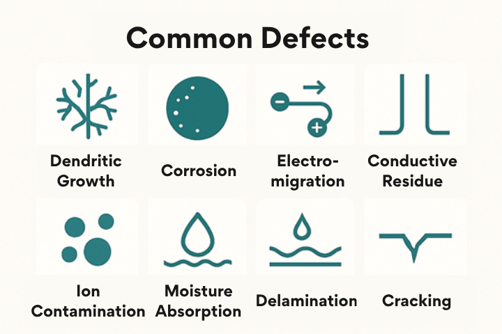
Understanding Surface Insulation Resistance Failures: Key Defects That Lead to Test Failures
When it comes to electronics reliability, surface insulation resistance (SIR) testing is one of the most important, yet often overlooked, safeguards. Failures in SIR can lead to mission losses,
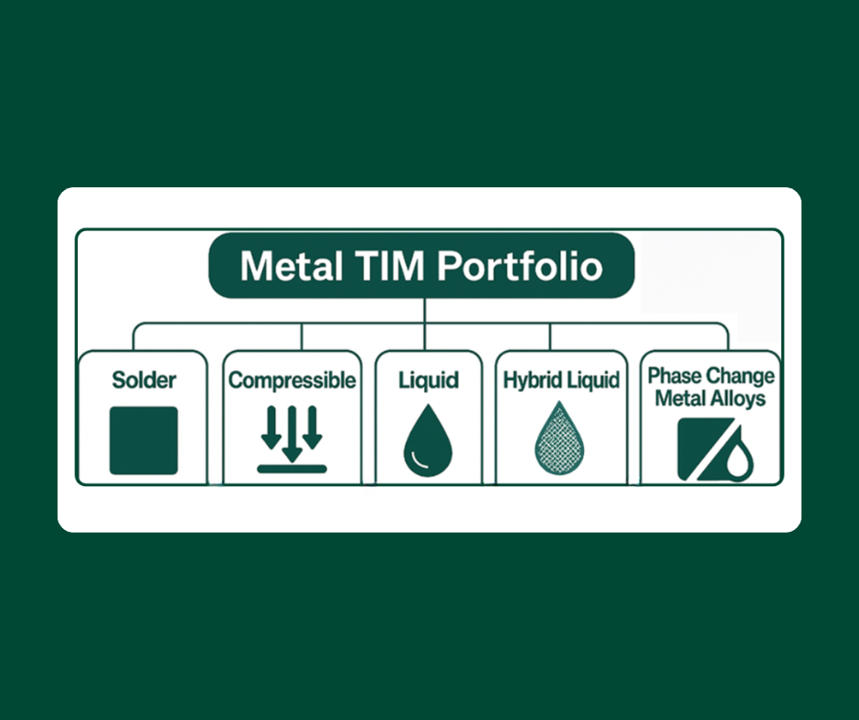
Innovative Metal Thermal Interface Materials for Bare Die AI GPU Server Processors and ASICs
Innovative Metal TIMs for AI/GPU Processors As artificial intelligence (AI) and high-performance computing (HPC) technologies evolve, their computational demands have skyrocketed, leading to a
From Texas to Utica: Finding Strength in Change
Embracing the Unknown When I received my internship offer from Indium Corporation in March, I was ecstatic. As a graduate student pursuing Industrial and Systems Engineering at Texas A&M
Winning Strategies: How Athletics & Internships Share a Blueprint for Growth & Success
While my experience in a traditional office may be limited, my time on the lacrosse field, in the weight room, and in scouting and coaches’ meetings is anything
Not sure what you need?
Let us help.
At Indium we research, develop, and manufacture advanced electronics assembly materials solutions to the challenges of today, tomorrow, and the future.