In a past entry, I discussed the characteristic formation of surface oxides on indium and the various methods by which to remove these to achieve a soldered indium interface. A related property of indium is its ability to cold weld to itself. The value of this for a thermal interface application is that it can essentially form a hermetic solder joint using ambient conditions, even supplying coverage over large surface areas.
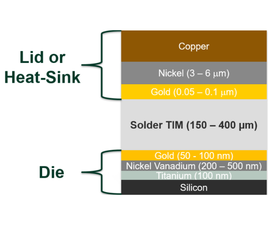
To perform this task, indium must first be applied separately to the two joining surfaces. Fluxes may be used for this attachment, but their residues can be completely cleaned off prior to the next step. Other indium attachment methods include sputtering or plating.
Once each surface is pre-wetted with indium, the indium surfaces are etched by chemical etching with a mild acid or plasma etching. Immediately following these indium etches, the two indium surfaces can be brought together to touch, and they will cleanly cold weld together.
This is not a new procedure, but one which is commonly overlooked as a thermal attachment method. Other processes such as semiconductor flip chip bonding are known to use the indium cold welding process to attach indium bumped chips (bumped during the last step of the photolithography processing of the wafer) to indium-plated, sputtered, or CVD-deposited pads.


