Indium corporation is now producing tin at very high purity – see here: https://www.indium.com/products/metals/tin/ –and I'd love to explain why we have invested in this technology:
Every new generation of silicon chips needs its Prometheus — the key technology that delivers the lower wavelength of light that is needed to print features onto a wafer. This sequence of steps has been used for decades and is known as lithography: Generate a bunch of photons and shape a beam that is bright enough, create the optical elements to steer the beam towards a feature-defining mask, project the resulting image on a wafer coated with photoresist, etch the pattern into the wafer, and finally strip the remaining resist away for the next process in the fab — it's not as easy as it sounds.
It is the reduction of the wavelength that lies at the core of this process, and we know the semiconductor industry has managed to do this many times because we have all heard of Moore's law.
So how exactly do you produce, with significant brightness, a beam of light at, say, 13.5 nm, that's necessary for 5nm and 3nm processes? Until recently, the answer had to be: "Easy — you use a synchrotron". These particle accelerators are available all across the world. Spoiler alert: There are only 60 of them, and only government funded research institutes have the means to build, staff, and operate them.
The next possible answer could be – "well — surely you can use a laser of some kind". The problem is that lasers at this wavelength are somewhat pricey as well. At 13.5 nm, we are looking at a "soft" X-ray kind of wavelength. Lasers are available,but still do not offer what is needed.
Enter then plasmas: You take a certain element, ionize it, and you get a plasma which emits light around a certain frequency that is unique to the element used. If you have ever looked through the window into an operating sputtering chamber, you have seen the purple glow emitted from an Argon plasma (see picture below).

Which finally brings us to back to tin: Light from a tin plasma has an emission spectrum around the 13.5nm peak that's needed. And, crucially, the tin plasma offers a high conversion efficiency that results in the high brightness required.
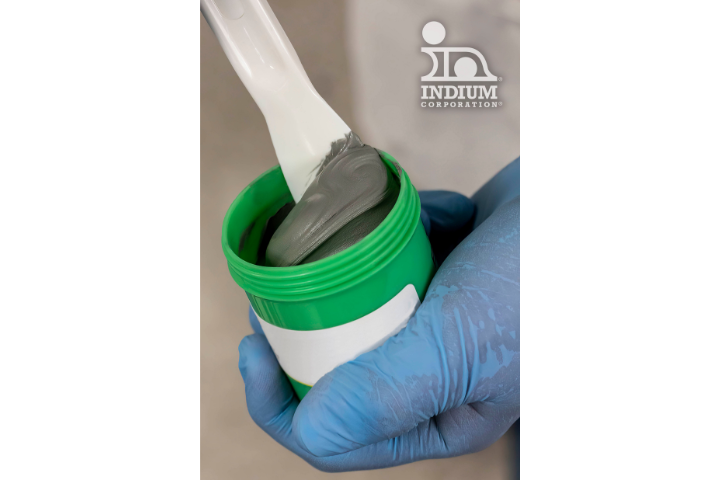
The other piece of good news is that tin is an element with a huge usage in today's world. In the electronics industry alone, it is used in the majority of solder alloys; here at Indium Corporation, we have been working with tin for a very long time.
We also have spent a number of years refining tin and pushing its purity beyond the standard degree available (4N, or 99.99%) to 5N and beyond to 6N, to create the purity level that is needed for this new application. Indium Corporation is ready to support this exciting new application that will play an essential part to keep Moores' law going for many years.