Many, many thanks to the hundreds ofyou who came by the Indium Corporation booth at Semicon West this year. Some of you came tohear about our recent global Semiconductor Assembly MaterialsRoadmap presentations, and allof youwanted to talk about your specific materials needs. Special thanks to those of youwho sharedthe many successes you are having with our growing portfolio of applications-specific materials.
Based on these discussions, justa fewof the topics that you will be hearing about in this blog in the coming months are:
– Lead/indium paste for multiple reflow applications onto gold pads
– Tin antimony solder paste
– Fluxes for 2.5D and 3D flip-chip applications
– Waferbumping fluxes for microbumps
– Jetting epoxy fluxes
– Tombstoning in semiconductor applications
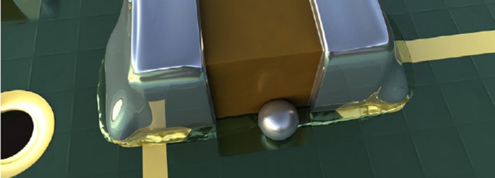
Also: a final big THANKYOUto our friends at Nordson/Asymtek for showcasing the Indiumhalogen-freePoP paste Indium9.88-HFwhich was still dispensing after over 3 days of continuoususage at room temperature: proving its hard-earned reputation as the Energizer bunny of Pb-free (lead-free) dispense pastes. Here is a picture from the final day.
We look forward to seeing you all in 2012 (Exhibits: July 10-12th, 2012).
Cheers! Andy