A more experienced engineer than myself offered a bit of advice for wafer bump plating with indium:
“Electroplating using the indium sulfamate plating bath is one method of depositingindiumbumps onto wafers. However, usingdirect current often results indeposits with a high degree of surface irregularitythat can result inelectrical shorts between individual bumps. One solution to the problem is to use microprocessor controlled pulse plating wherethe current polarity periodically changes, resulting in the plating and de-plating of indium. Obviously, the positive portion of the cycle where indium is deposited, has to be greater than the negative portion of the cyclewhere indium is de-plated, to have a net deposit gain.
Pulse plating works because the negative portion of the cycle removes excess indium in high current areas that plate faster than low current areas, resulting in a leveling or smoothing of the deposit. There are three variables in pulse plating:
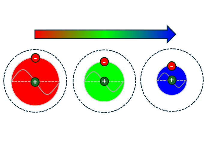
Wave shape – sine, sawtooth or square
Ratio of the amperageof the positive to negativecycle
Time on in both the positive and negative cycle
Determining these variables must be done empirically, and most companies that have successfully done so, consider the information proprietary.” We can suggest (offline) specific values asan initial starting point to establishing optimum settingsfor pulse plating of indium for a wafer bumping process.