Figure 1: 15% Voiding with air reflow

Figure 2: ~0% Voiding after vacuum reflow
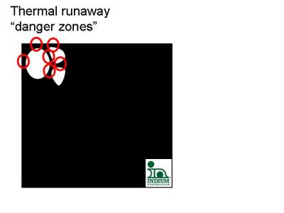
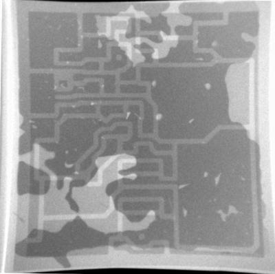
Figure 3: Multiple voids
While at the Semicon West 2009 show in July, I had a chance to sit down with Herr Klaus Roemer of Pink GmbH. PINK is most famous in the die-attach and power module manufacturing world for their reflow ovens with vacuum, but are also known in the medical and aerospace industries for manufacturing extremely high precision, one-off, vacuum equipment for applications as diverse as particle-accelerators for ion bombardment, and large-volume chambers for helium leak-detection. I asked him some questions about Pink vacuum soldering technology.
ACM: Why do people use vacuum soldering?
Klaus:
Shrinking package sizes and higher power density in electronic devices necessitatevoid-free soldering. Voids reduce the electrical and thermal conductivity and cause hot spots, which are very critical especially in the case of power electronics. The pressure in voids is usually around 1bar (ambient pressure). A vacuum of < 5 mbar (4 Torr) in the soldering chamber causes a differential pressure between the voids in the liquid solder and outside the solder connection, resulting in a force that effectively "pulls out" the voids against the resistance of the solder viscosity. Figures1 and 2 show the dramatic difference in voiding on a direct-bonded copper baseplate for an IGBT module.
Shrinking package sizes and higher power density in electronic devices necessitatevoid-free soldering. Voids reduce the electrical and thermal conductivity and cause hot spots, which are very critical especially in the case of power electronics. The pressure in voids is usually around 1bar (ambient pressure). A vacuum of < 5 mbar (4 Torr) in the soldering chamber causes a differential pressure between the voids in the liquid solder and outside the solder connection, resulting in a force that effectively "pulls out" the voids against the resistance of the solder viscosity. Figures1 and 2 show the dramatic difference in voiding on a direct-bonded copper baseplate for an IGBT module.
ACM: Don't other manufacturers also produce vacuum soldering equipment?
Klaus: Yes, we have some very capable competitors, but they usually can only solder with high temperature and preforms only, and not with solder paste. PINK has a unique patented technology which offers the following significant advantages:
· Void-free soldering in inline systems for mass production or batch type ovens
· Soldering with solder paste (highly efficient flux management system) and / or soldering with preforms
· Flux free soldering possible, by using formic acid or forming gas
· Temperature profiles in accordance with IPC / JEDEC or customers specifications, with a short process time of typically 6 minutes only
· Adjustable and controlled temperature gradients
· Process temperatures up to 400°C
· Consistent process control and traceability
ACM: How does PINK manage the fast heat transfer required for precisely controlled heating and cooling?
Klaus: In each heating zone within the oven, a large block with a high thermal mass is heated to a constant temperature, and is then raised to touch the platen on which the substrate is resting. The number and the time period of "touches" of the thermal mass against the platen dictate its temperature and heating gradient, allowing a very precise profile control, using a PID-controller feedback-loop. Cooling is done the same way, with a vice versa heat flow. An efficient flux- management system in the "VADU" by PINK allows 24/7 production. Liquid flux residues can easily be removed by just opening taps in the flux collection reservoirs. Burning of flux residues is prevented by using a spike reflow temperature which is only about 20°C higher than the soldering temperature.
Our Youtube video shows this process very well. You can see the "bubbling and boiling" of the reflowed solder paste, as flux volatiles expand under the die, and outgas.
Voids are typically found to be less than 1%, often zero and although many customers always ask for always "zero voids" this is difficult to achieve, due to variations in the substrate and die finishes.
ACM: Klaus, das war sehr interessant! Danke für die Informationen.
—
Andy Mackie comment:
Don't forget that each time that a void appears under a die, it increases the current density (A / cm2) as an inversefunction of the void cross-sectional area. In a situation where there is a lot of voiding, this can lead to thermal runaway. For example (figure 3) in the case of a junction between several voids, the thin films of solder between the voids may heat up to higher temperatures, as the voids will not conduct heat. This becomes a vicious cycle, where the hotter film of solder has a lower resistance, so carries more current, so gets heated up more, and so on, and in some instances the die may actually be "blown" off the direct bonded copper substrate by the pressure in the expanding void, combined with the weak or even molten solder.
Cheers! Andy