Wafer bumping processes have evolved in the last 10 years. The semiconductor assembly industry has gone from bumping processes using solder paste printing (with all its concerns of voiding, coplanarity, stencil-life, and spatter) to plated solder bumps, and now to plated copper pillars with microbumps (solder endcaps). as shown in figure 1.
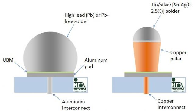
Figure 1: Evolution of Flip-Chip Bump Metallization and Structure
The reasons for the move from standard solder bumps to copper pillars are primarily to:
- allow high I/O ultrafine pitches (<80microns) without solder bridging
- maintain high stand-off (chip – substrate clearance) to reduce stress on the chip surface
- eliminate or reduce electromigration issues caused by current crowding in solder near the UBM
The basic process flow for copper pillar/microbump formation is shown in Figure 2.
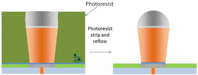
Figure 2: Copper-Pillar Solder: from plating to finished microbump
To eliminate voids in the final reflowed joint, it is critical to have a reflowed solder microbump surface that is perfectly hemispherical, smooth, organic- and inorganic-residue free, and coated with a thin semi-passivating layer of tin monoxide. There are two instances in which the solder bump or microbump must be reflowed:
- after the photoresist and seed layer are stripped, the rough electroplated bump is contaminated by various oxides and hydroxides of tin (from reaction with the highly corrosive resist strip material), plus organic debris entrapped in the rough plated bump surface.
-
if the wafer is probe-tested in a way that coins (damages) the top of the solder bump, this bump may also need to be re-reflowed to return it from its coined condition to a pristine hemisphere. This eliminates coin-related voids in the subsequent flip-chip joint.
I will be going into more detail on the usage of specialty wafer bumping fluxes and critical aspects of process control to generate pristine microbumps, in a subsequent set of blog posts.
Cheers!
Andy