Hello all,
As mentioned in my recent posts, I’ll be presenting a webinar soon on solder paste printing for system-in-package (SiP) applications. Contrary to the title, printing won’t be the only thing I’ll talk about. One important topic that doesn’t directly involve the printer but is a natural follow-up process is solder paste inspection, or SPI. I say it is the natural follow-up because there needs to be a way to actually measure solder deposit height and volume after a print to determine if there are any defects. Identifying these defects lets a person go back to the printer and adjust the appropriate parameters to work towards a solution.
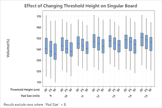
Indium Corporation recently installed a new SPI machine that has a much higher resolution than its previous model, perfect for analyzing solder paste for SiP applications (as I wrote that sentence, I was reminded of how careful I need to be to not mix up “SPI” and “SiP”). One of the parameters that I’ve learned is important for SiP applications is the threshold height, which is the limit beyond whatthe machine will report an error for excessive height (and calculated volume). As you can imagine, for SiP applications, the threshold height needs to be very low, in the realm of tens of microns, as the stencils used are very thin. As such, precise calibration of threshold height is necessary for accurate measurement.
Take a look at the graph below as an example. The x-axis shows changing threshold height settings, increasing from 20 to 30 microns, and the effect that change has on the volume % of various size pads on the same printed board. As you can see, even a five micron change in threshold height has a noticeable effect on the reported volume % of a pad. That change could be the difference between a pad being reported as a defect or not, so it’s important to ensure that the threshold height parameter is calibrated correctly.
There are more parameters to consider with respect to SPI when it comes to SiP printing. Tune into the SiP Printing 101 Webinar if you’re curious and want to learn more!