(See Part 1)
When discussing success in solder paste stencil printing for SMT assembly, one of the most important tools in an engineer‘s “belt” is his solder paste inspection (SPI) equipment. This is especially important for smaller stencil apertures/paste deposits that are difficult to see with the naked eye, at least for an older gentleman such as myself. Knowing that there is solder paste on the pad is important, but consistency from pad to pad is critical. There are two important metrics to consider in measuring a printing processes success: the area ratio and transfer efficiency. The area ratio determines the potential for success; transfer efficiency quantifies success by comparing the volume of the aperture to fill to the actual fill of the aperture, as measured by SPI.
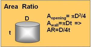
Figure 1
Area ratio (AR) is a critical metric for successful stencil printing; it is the area of the stencil aperture opening divided by the area of the aperture side walls. Figure 1 shows a schematic for a circular aperture. A simple calculation shows that the area ratio (AR) is the diameter (D) of the circle divided by 4 times the stencil thickness (t): AR = D/4t. The same formula is used for square apertures, with D now equal to the side of the square. For the AR of a rectangular aperture, the formula is a little more complicated: ab/2(a+b)t, where a and b are the sides of the rectangle. The industry widely accepts that, in order to get good stencil printing, the AR must be ![]() 0.66. Experience has shown that, if AR < 0.66, the transfer efficiency will be low and erratic.
0.66. Experience has shown that, if AR < 0.66, the transfer efficiency will be low and erratic.
Transfer efficiency, another important stencil printing metric, is defined as the actual measured volume of the solder paste deposit divided by the volume of the aperture. As already mentioned, the most important tool to measure the efficiency of the stencil printing process is a SPI machine. SPI equipment can be utilized to detect insufficient or excessive solder paste deposits and to determine if the solder paste deposit is located squarely on the PWB solder pad.
Hence, SPI enables accurate decisions about the volume and position of the solder paste deposits. Such data can eliminate subjective and, perhaps, erroneous decisions from the decision making process. The SPI data can also alert the process engineer to stencil printing issues that otherwise may be overlooked.

Figure 2
An example of stencil printing results can be seen in Figure 2. Three different solder pastes (Paste A, B, and C) were evaluated over various aperture sizes. Figure 2 focuses on 0402 solder paste print deposits. The transfer efficiency measured on the y-axis is in percent volume, giving a ratio comparing the volume of solder paste deposited divided by the actual volume of the stencil aperture. Obviously, 100% is the target as this means that the solder paste filled the aperture completely and 100% was released onto the PCB pad.
If one were to simply take the average of the data above, they might choose Paste C as the material of choice. Though volume is certainly important, consistency from pad to pad is also critical and sometimes overlooked. There are two graphs depicted; the lower graph reports the standard deviation of the data in the graph above it. Experts have suggested that as well as meeting the target (100% transfer efficiency in this case), consistency is also vital to success. A standard deviation of 10% or less equates to a consistent process. Of course, a process can be consistently poor (still have less than 10% standard deviation) but have very low transfer efficiency, so both graphs are imperative. In case you’re wondering, Paste A would be the material of choice in this instance as it is near the target (100% transfer efficiency) and consistent (close to 5% standard deviation in most instances).
Why is consistency important? A couple of examples may help explain. First, for discrete components, tombstoning occurs when there is a force imbalance at either end of the component. There are many reasons this force imbalance may occur, including, in this instance, when more solder paste is deposited on one pad than the other. In such a situation, an unequal pull is created as the solder coalesces, with greater force on one end of the component.
The second example involves a BGA-type component. Consider the situation where there are three consecutive pads in a row. If the two outer pads have significantly more solder paste deposited on them than the pad in the center, the potential for an open defect will significantly increase for the center connection.
Solder paste inspection equipment plays a huge role in our company’s solder paste design and evaluation process. It should play a significant role in your SMT assembly process, as well.
See Part 3. See Part 1.