Library
Blog
Topic
Type
Year
Author
Product Type
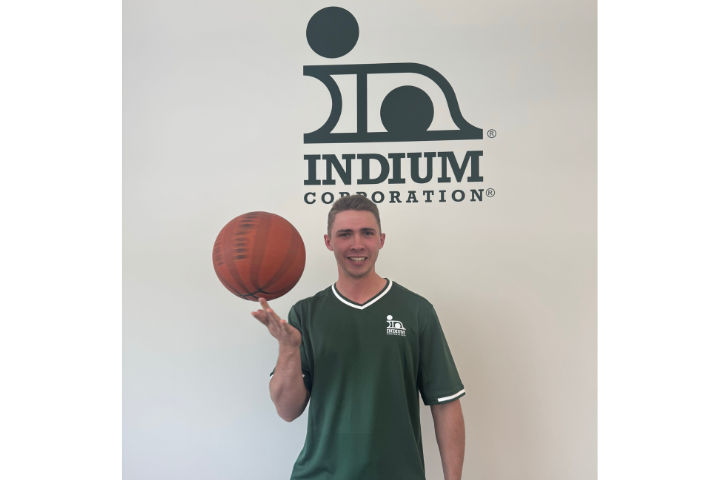
My Rocky Road to Human Resources
If you had told me 4 years ago that I would have a business internship in Human Resources, I would have probably laughed in your face. Fifteen-year-old me was convinced she was going to have a career
From Freud to Fringe Benefits
I started college as a general psychology major, as that was my interest. I wasn’t too thrilled with the idea of becoming a therapist or a professor. I just knew I had a love for people and the way
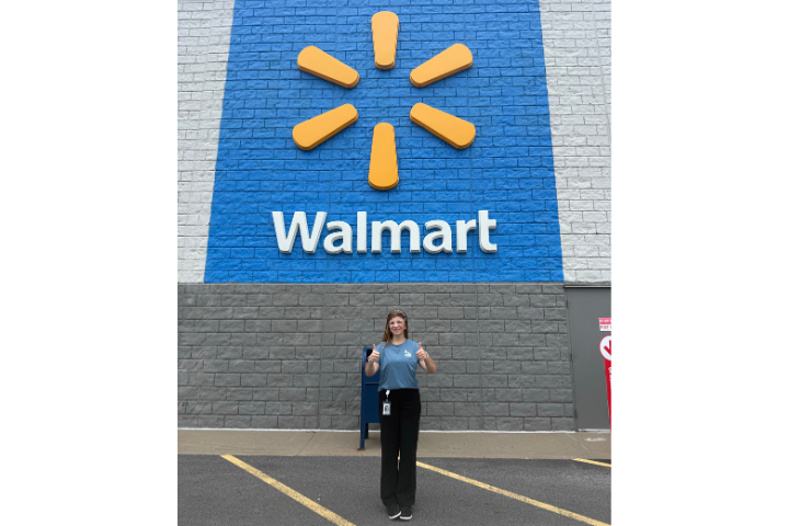
There’s More Than One Way to Get to Walmart
What’s your favorite thing about your hometown? Do you have an answer? Because when my freshman orientation leader asked us to introduce ourselves with our name, major, and something we love about
The Bigger Picture: Why Every Finance Professional Needs Business Awareness
Thinking about my short experience so far at Indium Corporation, the main thing that comes to mind is how significantly my perspective on the business world has changed. Coming into this internship,

The Best Way to Approach a Problem
Problems are a part of everyday life. Whether in school, engineering, manufacturing, business, or personal situations, challenges come up that require thoughtful solutions. The difference
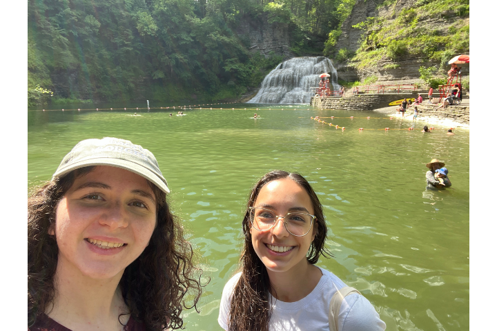
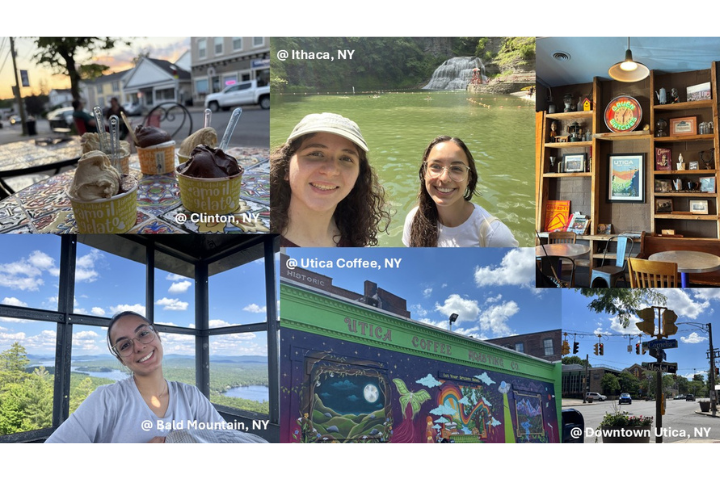
Community: From the Office to the Dorms
Before starting my internship, I was worried about moving to an unfamiliar new city. I didn’t have an established group of friends or knowledge of the area that I could lean on as I transitioned
The Importance of the Community Around You When Taking the First Steps in the Workplace
Taking your first steps in the workplace, in your career, feels just like taking your first steps in any other milestone, such as kindergarten. As a sophomore at the University of Notre Dame, I
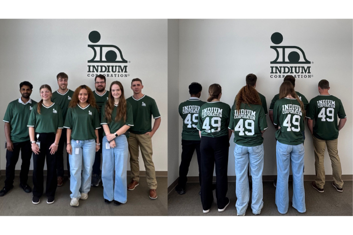
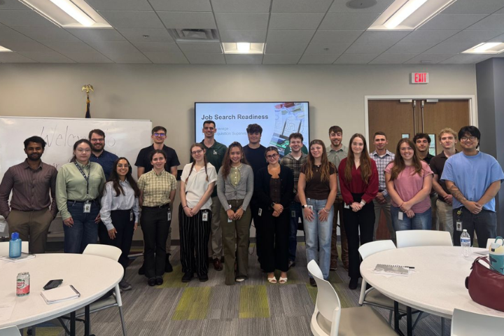
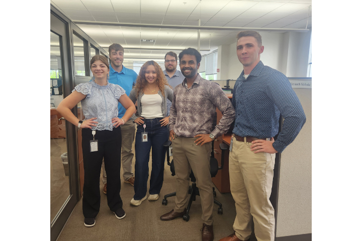
The Internship Moment No One Posts on LinkedIn
If you search “internship” on LinkedIn, you will probably see the same things over and over again. The first day picture. The “excited to start this new chapter”
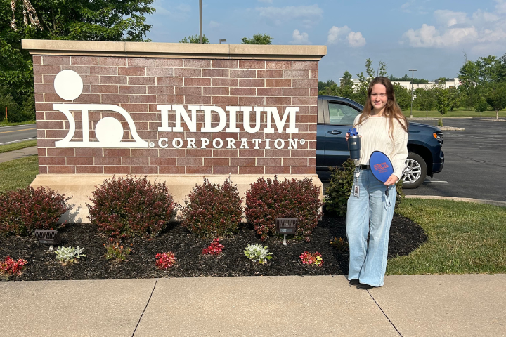
The Human Side of Indium Corporation: Lessons, Laughter, and Mentorship
When I received my internship offer from Indium Corporation, one of the first things I did was open LinkedIn and see if I had any mutual connections at the company. I found exactly one person. I will

Communication with Colleagues and How This Work Environment Compares to Past Jobs
Beginning my internship at Indium Corporation has been an exciting and rewarding experience. Every day presents an opportunity to learn something new, whether it is developing a technical skill,
No Beginning Expectations, No Problem
Introduction When stepping headfirst into this internship, I had no idea what to expect. I have never had a true engineering internship in a full office setting before. When applying at the
Nerves, Strengths, and Stories: My Path to Building Confidence and Making Connections
Coming into this summer at Indium Corporation, I had a few key goals in mind to make the most of this internship. So far, technical goals, such as developing new lab skills and obtaining a greater
Food for Friendship: Intern Lunches and Dinners Shaping Friendships
Eating is necessary to live: it is one of the simple truths of being a human. Yet, there is more to meals than just basic survival. Sharing a meal with someone is one of the more common sources of
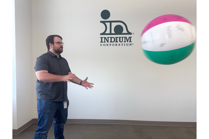
Beach Balls & Gelato: Building Connections and Facilitating Career Growth Pt. 1
Beach Balls & Gelato: Building Connections and Facilitating Career Growth Pt. 1 Let me start off by laying this out – one of the most important experiences you can have while in college is not
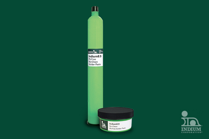
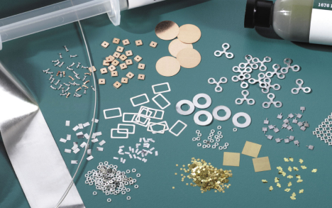
Good Solder Paste Response-to-Pause Increases Profability Part 2
Folks, Let’s check in on Megyn Woodley as she helps Andover Electronics solve their response-to-pause problem… Megyn Woodley had performed response-to-pause experiments on the solder paste that
Good Solder Paste Response-to-Pause Increases Profitability Part 1
Megyn Woodly had just finished a three-day audit of Andover Electronics Assembly’s four assembly lines. She felt the factory was well organized, run with high first-pass yields, and quite good
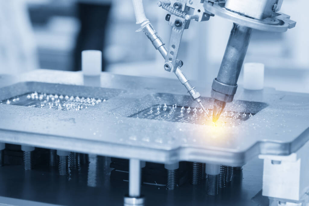
Robotic Soldering, Smarter (Part 3): Indium Corporation’s Innovation and the Future of Robotic Soldering
In Part 2, we outlined materials challenges that can impact robotic soldering performance. In Part 3, we shift to product solutions and emerging innovations—highlighting how cored wire performance
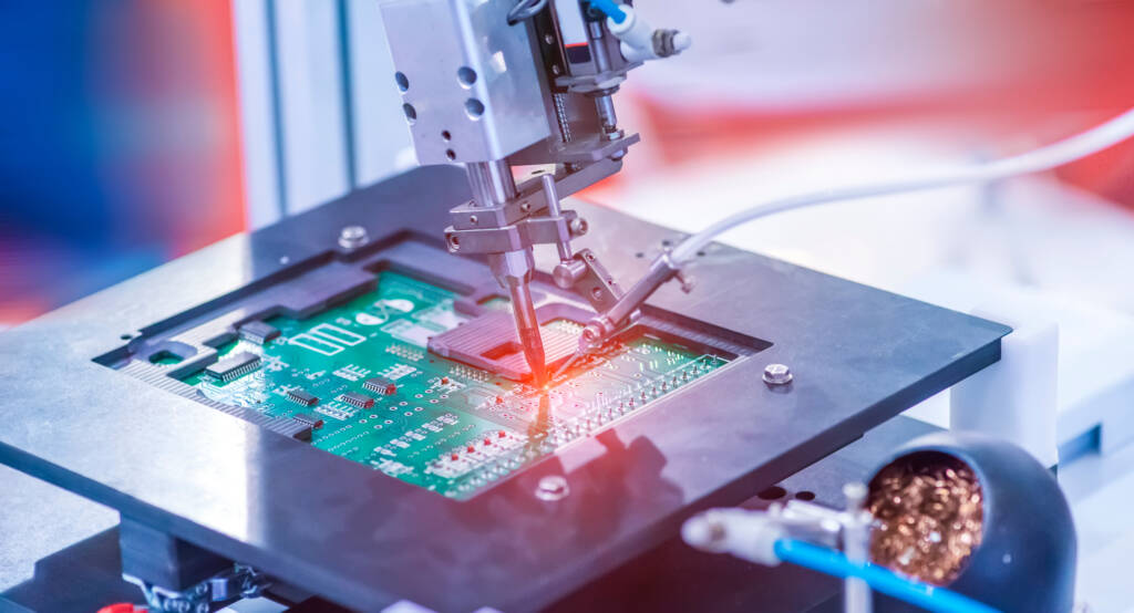
Robotic Soldering, Smarter (Part 2): Tackling Common Materials Challenges in Robotic Soldering
In Part 1, we covered how robotic soldering evolved, and why materials quality is a major driver of process stability and precision. In Part 2, we focus on common materials-related issues that can

Robotic Soldering, Smarter (Part 1): From Automation to Materials That Make It Reliable
Robotic soldering has evolved from a productivity upgrade into a precision requirement—especially as electronics become smaller, denser, and require shorter production cycles. In Part 1 of this
The Electron: A Biography and the Rise of Modern Electronics
Folks, In my last post, we explored the dawn of electricity and the early days of radio. Now, we move further along the history of electronics timeline to see how everyday consumer products forced
The Electron: A Biography and the Emergence of Soldering
Folks, My interest in the history of electronics was piqued when I attended a mid-1990s lecture by Noble Laureate Arno Penzias on the same topic. Penzias was a co-discover of the Cosmic Microwave
Not sure what you need?
Let us help.
At Indium we research, develop, and manufacture advanced electronics assembly materials solutions to the challenges of today, tomorrow, and the future.