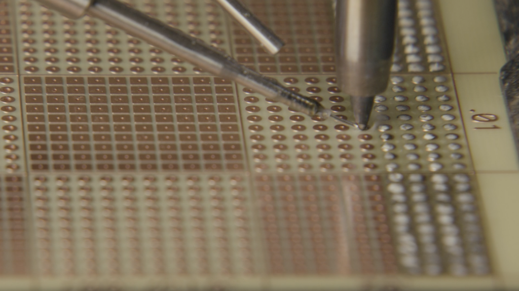
I really do mean art… This image was generated by Michael Riddle of Cyber Technologies for a project we are working on. Maybe I’m just crazy about this kind of thing, but I wouldn’t mind having this hanging on a wall in my house – it’s just cool!
Mike let us in on how to create these very descriptive images:
“We call the process of separating deposited materials from the substrate “Surface Subtraction”. The steps are easy to follow:
1) Fixture and scan the bare substrate (Scan A)
2) Deposit the material to be measured
3) Re-fixture the printed substrate and re-scan, using the same settings as Scan A. We will call this scan “Scan B”.
4) In our software we can subtract one scan from another. We call this feature “User-defined Compensation” .Here, we subtract Scan A (the bare substrate) from Scan B (the printed substrate) leaving only the deposited/printed material.
For the 3D image, I first plotted the 3D surface map of the bare substrate, and then plotted the 3D surface map after the user-defined compensation was enabled.”
Data is the output that we initially look forward to, although tech presentations need some ‘spice’, and this type of creative tech art can really drive home the point you are trying to make with your data.


