Ultrasonic Testing (UT), performed by acoustic microscopy, is a great way to determine the quality of a solder bond without destroying the assembly.
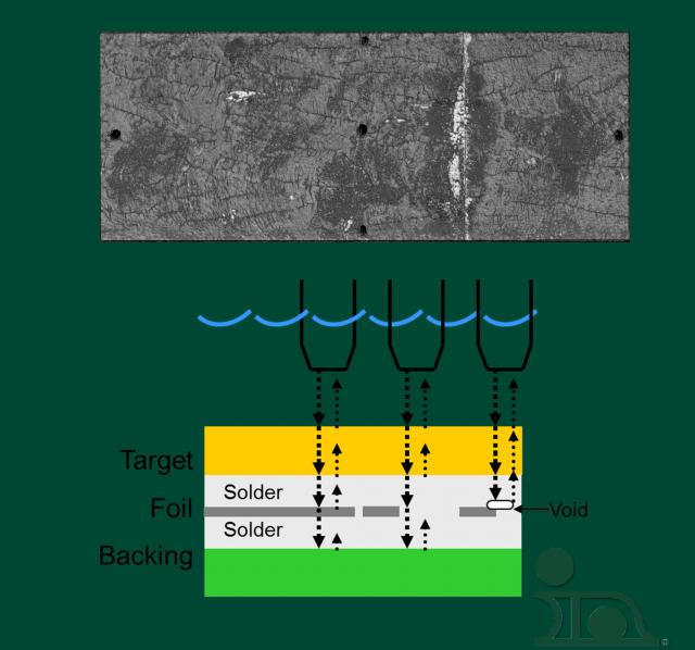
As a very basic description, SAM (scanning acoustic microscopy) uses sound waves to travel through the assembly, much like some animals use sonar to locate objects. Sound waves generated by a transducer travel through the assembly and bounce back when they encounter different materials. Air reflects back much differently than metal, so, by using sound waves, we can locate pockets of air (voids).
In a NanoBond® you can expect to see 2 things:
1) darker spots where the NanoFoil® is located in the bond and
2) very little voiding, which will appear as white areas. Here is an example of voiding:
Most of the time we see little or no voiding. We typically achieve <2% when we bond sputtering targets with NanoFoil® in-house. Here is an example:
If you have experience with traditional large area soldering methods, you will notice that <2% voiding is a sign of a very good bond.
For sputtering targets this is necessary to reduce pump-down times and eliminate ‘virtual leaks’. Contact us if you are interested in learning more.
*This post is part of the NanoBond® Process series


