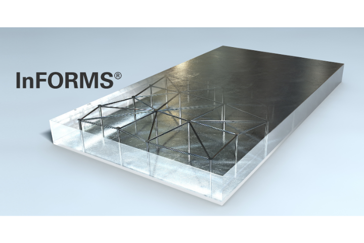
Indium oxidation is not merely a surface phenomenon—it plays a critical role in the performance and reliability of high-precision applications, including semiconductors, AI, high-performance computing, and data centers. Given its exceptional thermal conductivity, malleability, and reliability, pure indium is indispensable as a solder thermal interface material (sTIM) and solder preform. Controlling and measuring the oxidation layer is vital to preserving these qualities and ensuring optimal performance.
This blog explores the impact of indium oxidation, effective ways to measure oxide thickness, actionable solutions to minimize the effects of oxidation, and highlights the value of a collaborative approach in advancing industry standards.
Why Indium Oxidation Analysis Matters
While indium’s natural properties make it an ideal material for sTIMs and solder preforms, oxidation can compromise its reliability, purity, and performance. A thin layer of indium oxide, typically a few nanometers thick, naturally forms on its surface when processed into preforms. Indium preforms are self-passivating, meaning that when exposed to air, a thin indium oxide (In₂O₃) layer will form. This layer acts as a barrier, which protects the underlying indium from further oxidation. Though self-passivating and protective under stable conditions like climate control, appropriate packaging, and being handled responsibly, this oxidation can affect indium in critical ways:
- Degraded wettability and bonding: Oxide layers inhibit indium’s ability to adhere to surfaces. This results in reduced solder bond strength and increasing the likelihood of voids.
- Higher electrical resistance: Oxidized layers act as insulators, leading to inefficiency and potential system failures.
- Reduced thermal conductivity: Indium’s prized heat transfer capabilities can weaken due to insulating oxide barriers, risking overheating in sensitive components.
- Handling challenges: Oxidized indium can become brittle, flake, or fracture, impacting manufacturing yields.
For applications like data centers, AI systems, or high-powered computing, in which thermal and mechanical reliability are paramount, even minor oxidation can result in system failures, reduced performance, or costly repairs.
Measuring Oxide Thickness on Indium Preforms
To confirm premium materials are being used, it becomes important to develop precise measurement techniques. Below are the leading methods for evaluating oxide thickness, highlighted alongside their benefits and challenges.
1. SEM/EDX (Scanning Electron Microscopy with Energy Dispersive X-ray Spectroscopy)
This combination provides high-resolution imaging and elemental analysis, ideal for detecting oxygen presence and oxide-layer characteristics.
- Advantages:
- High-resolution images for detailed surface composition
- Quick results with minimal sample preparation
- Elemental and spatial mapping
- Limitations:
- Ineffectiveness in detecting light elements
- Dependence on a vacuum environment
- Limited depth profiling capability
By creating precise visual maps of surface topography, SEM/EDX enables rapid assessment of oxidation impact on preforms.
2. FTIR (Fourier Transform Infrared Spectroscopy)
FTIR identifies surface oxide layers by analyzing how infrared light interacts with a material. Its non-destructive nature ensures samples remain pristine.
- Advantages:
- Non-invasive, preserving sample integrity
- Broad material compatibility
- Fast and repeatable for consistent results
- Limitations:
- Reduced precision on metallic surfaces
- Complex spectra interpretations
- Sensitivity challenges for trace elements
Despite limitations, FTIR excels in scenarios requiring repeatable, large-scale oxide evaluations.
3. XPS (X-ray Photoelectron Spectroscopy)
For those seeking detailed oxygen concentration data, XPS is the pinnacle of surface analysis techniques.
- Advantages:
- Surface-specific precision with chemical state information
- Offers quantitative and wide-ranging elemental data
- Non-destructive and depth-profiling capable
- Limitations:
- Cost-intensive and time-consuming
- Sensitive to vacuum-induced material changes
- Limited effective area of analysis
The trade-off for XPS is its ability to map oxidation under controlled environments with unmatched depth and clarity, making it invaluable for long-term research and development (R&D) projects.
4. Spectroscopic Ellipsometry
Widely used for thin-film measurement, ellipsometry gauges oxide thickness by analyzing the change in reflected or transmitted light polarization. This approach is sensitive and provides multi-layer profiles under optimal conditions, making it Indium Corporation’s preferred method for measuring indium oxide layer thickness.
- Advantages:
- Non-contact, preserving material conditions
- High sensitivity for ultra-thin oxide layers
- Comprehensive optical property analysis
- Limitations:
- Requires smooth surfaces for accurate results
- Relies on detailed material models
- Limited direct chemical composition insights
By addressing variables like surface irregularity, ellipsometry becomes a powerful tool in tackling oxide-layer complexities.
Covalent Metrology Collaboration Insight
We worked with Covalent Metrology in Sunnyvale, California, to develop a measurement technique for thin oxide films using spectroscopic ellipsometry.

Shown above are test results: nine samples of a 99.99 purity indium preform were tested for oxide layer thickness post-manufacturing. This was compared to nine samples of a 99.99 purity indium preform subjected to 48 hours of aging in air environment at 140°C. These results were obtained using a spectroscopic ellipsometry based methodology developed through our collaboration with Covalent.
Although layer thickness measurement is a routine application of ellipsometry, measurement of oxide thickness on metals comes with unique challenges. A standardized test procedure has been developed specifically for indium surfaces and has been shown to work well through rigorous testing. Ellipsometry is a non-destructive measurement technique that measures changes to the polarization state of a measurement light beam to determine material optical properties and layer thicknesses. The test procedure we’ve developed with Covalent is customized to the specific properties of indium and its surface oxide, and is designed with robust statistical sampling to allow accurate oxide thickness measurement for ongoing preform production. Compared to alternative oxide thickness measurement options, such as XPS, this new ellipsometry-based inspection delivers far larger datasets at lower cost.
Overcoming Challenges with Spectroscopic Ellipsometry Measurement for Indium Native Oxide Layer Thickness
Spectroscopic ellipsometry is an optical measurement with its own set of variables that need to be accounted for. Below is a result in measurement variation on the same preform. The results in blue are striations pointed parallel to the beam of light shined upon it, while the results in red are striations pointed perpendicular to the beam of light. If the surface roughness or irregularities vary too much, the light reflected off the surface may not give the expected results. It’s important to ensure the surface is as smooth as possible for this measurement technique.

Below is a comprehensive study of pure indium preforms manufactured using different forming processes, to see how these process variations affect indium oxidation rates. Spectroscopic ellipsometry acted as a great quality check for the planarity and flatness of the preforms. Each preform was measured at the same locations, from the center of preform and two opposite corners. Each preform also was measured with striations parallel and perpendicular to the ellipsometer’s light to detect any variation in the oxidation measurement. For each location measured, 25 data points were taken within a 1 cm x 1 cm area to map out the model’s oxide layer thickness measurement.

All preforms tested had ~10 nm maximum oxide layer thickness or less, which follows our previous data trends and existing literature on indium oxide layer thickness in standard temperature conditions.
It should be noted that the model was notadjusted between the previous irregularity testing and processes A-C of this study. All data collected prior to the surface irregularity dataset agreed with Indium Corporation literature’s 4-10 nm native indium oxide layer thickness. By keeping the model consistent, it proved that this sample was different from other samples due to its higher surface roughness. This also proves the model could be used for manufacturing or processing impact studies that could impact sTIM’s soldering performance.
Please note that industry-wide measurement of indium oxide layer thickness is typically not a readily-available process. Model fitting depends on the surface roughness of the preforms and the consistency of your manufacturing processes.
Minimizing Oxidation for Enhanced Purity
While measurement is vital and shows us that, in most ambient conditions, indium will self-passivate and only form a thin oxide layer, it is still important to take preventative steps to preserve the indium preform’s integrity. Below are our best recommended practices for storing and handling indium preforms for manufacturing and developmental work:
- Optimal packaging and storage conditions:
- Store indium preforms in vacuum-sealed, moisture-barrier bags filled with inert gases like argon, or in an inert environment like a cabinet.
- Use tape & reel or tray packaging to minimize exposure to air.
- Handling and assembly practices:
- Avoid bare-hand contact and handle with precision, using clean environments and proper PPE.
- Re-seal remaining preforms in nitrogen cabinets when not in use.
- Environmental controls:
- Maintain low humidity and temperature-controlled environments during manufacturing and assembly.
- Use preforms promptly after unpackaging to reduce oxidation risks.
By integrating these steps into manufacturing and storage workflows, businesses can extend indium’s shelf life and usability, ensuring pristine quality during application.
The Bigger Picture: Real-World Applications and Future Innovations
Indium oxidation, while a naturally occurring process, poses significant challenges to industries that rely on indium’s exceptional thermal and mechanical properties. In the semiconductor, AI, high-performance computing, and data center sectors—where thermal efficiency, solderability, and long-term reliability are mission-critical—even nanometer-thin oxide layers can introduce variability that jeopardizes system performance.
Uncontrolled oxidation degrades indium’s wettability, increases electrical and thermal resistance, and impacts mechanical stability. These effects translate into poor thermal contact, reduced sTIM effectiveness, and ultimately, increased failure rates in devices and systems operating at extreme power densities.
By deploying advanced, non-destructive measurement techniques like spectroscopic ellipsometry and implementing strict packaging, handling, and environmental protocols, manufacturers can minimize oxidation, ensure consistent bonding, and maintain peak thermal conductivity. The result is a more stable, high-performing sTIM solution that supports innovation at the heart of AI acceleration, chip-scale integration, and data infrastructure growth.
Through proactive oxidation control and precision manufacturing, the industry is better equipped to meet the demands of next-generation technologies with confidence and consistency.
Explore Tailored Solutions with Indium Corporation
Accurate indium oxidation analysis is crucial for maintaining reliability across high-precision applications. With robust monitoring and control, semiconductor manufacturers and high-performance computing sectors can ensure peak operational efficiency and longevity.
For a more in-depth understanding of oxidation and the reduction behavior of pure indium, read “Thermodynamics and Kinetics of Oxidation and temperature Dependent Mechanical Characterization of Pure Indium Solder” by Harry E. Schoeller of State University of New York at Binghamton.
Discover how our advanced materials and metal sTIM expertise provide unparalleled support in managing indium oxidation. To learn more, connect with a metal sTIM specialist or visit our thermal interface material page.
Together, we can pave the way for sustained innovation and precision.