Just before the APEC show, I discussed a new assembly technology in which Indium Corporation has been seeing commercial success, with my friend and colleague Seth Homer.
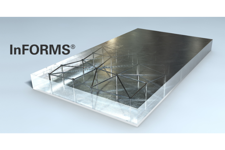
Andy: Indium Corporation introduced the InFORM® at PCIM in Nuremberg Germany back in 2016, and we featured it at APEC last year. We will do again this year. We’ve seen a considerable amount of adoption for this product ever since. What is the InForm?
Seth: It is a metal support matrix encapsulated in a solder preform. Think of it as a composite material, the relationship between the non-reflowable matrix and the surrounding bulk solder complement each other to provide strength and bondline planarity. It combines the “near net shape” effect that you would see in a pressureless sintering material, with the reliability of a solder joint. The best of both worlds, the solder and the matrix work together to provide a more consistent and a more durable bond, enabling improved reliability.
Andy: Why are customers adopting it?
Seth: The InFORM is designed to offer planarity control. Since the matrix doesn’t reflow, it provides a consistent predetermined stand-off height. This planarity control mitigates both corner stress concentration and current and thermal inconsistency.
As current densities increase, major issues are emerging:
- Thinned die: making die warpage and breakage during pressurization a concern
- Substrate roughness, die bend
- Coplanarity:
- Voiding:
Pressurized sintering may also be effective, especially for die-attach, but achieving consistent pressure on the die across the whole working area, and also across the die (zero tilt), is a challenge.
Unlike sintering, the reliability of the final InForm solder joint is much less sensitive to the condition of the surface, as the formation of the final joint is driven by the free energy of formation of intermetallic formation, not by a simple diffusion of surface metal atoms.
Andy: What device types will benefit from InForm technology?
Seth: The InForm was originally designed to be used at the system solder level, between the baseplate and the substrate. We now offer solutions atthe die level as well.
Andy: How is the InForm applied and used?
InForms are supplied in tape & reel packaging, and are primarily soldered in a vacuum reflow process using formic acid. We can also offer them flux coated for Ni or Air reflow. They are a drop-in replacement for standard solder preforms.
Lastly, the InFORM can help with design tolerance challenges by offering dependable standoff dimensions. Package designs are getting smaller and power densities are increasing. To combat the heat concentration, methods which help remove heat, such as double sided cooling, are being considered. This will require more stringent dimensional tolerances in the design.
Andy: As Power Semiconductor evolves, do you see a role for this technology in integrated power devices (IPD)?
Seth:Definitely. The benefits of this product will address design challenges that aren’t going away anytime soon.
Andy: Many thanks, Seth.
We hopesee you all at APEC!
Cheers Andy


