Folks,
This post is an excerpt fromIndium Corporation's The Printed Circuits Assemblers Guide to Solder Defects.
Introduction
Printed circuit board (PCB) issues can be a challenge, but not all of them can send your PCB to an early grave like tombstoning. Tombstoning is caused by unequal surface tension forces created during the melting of solder paste on opposite sides of a passive component. These unequal forces cause the passive component to lift up on one end and break contact with the circuit, resulting in something that looks eerily similar to a tombstone in a graveyard (see Figure 1).
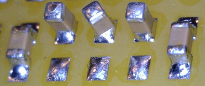
Figure 1: Tombstoned capacitor components.
Tombstoning Mechanism
Various factors contribute to tombstoning. Tombstoning is almost always the result of uneven wetting forces on the terminations of the component. When one end “wets” before the other, the now unbalanced wetting force of the solder “pulls” the component and rotates it, causing it to stand on end. We also encounter tombstoning following uneven heating of the PCB assembly. As the printed wiring board (PWB) travels through the reflow oven, the leading side of the passive component is often heated first (see left side of passive in Figure 2). This uneven heating causes the solder paste deposit closest to the heat source (the left side of Figure 2) to melt first. As this solder melts, its surface tension causes the passive to stand upright as seen in Figures 1 and 2.
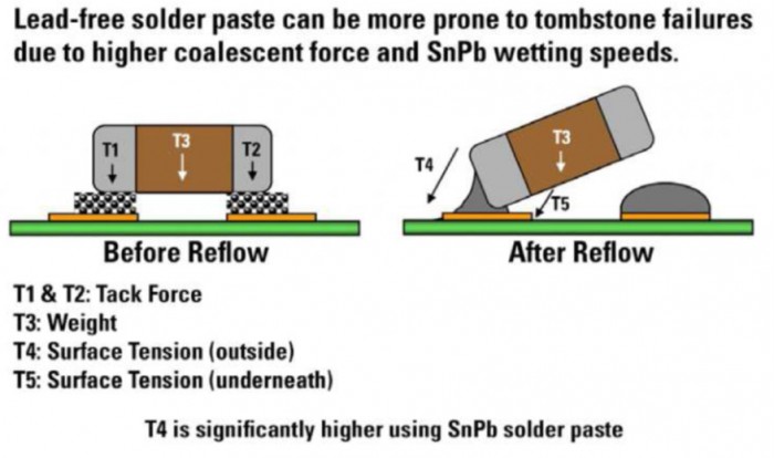
Figure 2: The tombstoning mechanism in detail.
Solder Alloy
One approach to minimize tombstoning is to use a solder alloy that has a large “pasty” or “plastic” range as it melts. The plastic range is the range of temperature over which the solder is molten and solid. For a eutectic solder, such as Sn63/Pb37 solder, there is no plastic range, as the solder is completely solid at just under 183°C and completely liquid at just above 183°C. SnPbAg alloys, such as Sn62 or Indalloy®100, have been widely used to eliminate tombstoning issues with leaded assemblies due to their increased plastic range.
In Pb-free solders, SAC3510 (Sn/3.5Ag/1Cu) has a narrow plastic range, whereas SAC305 has a broader range. Therefore, one would expect SAC305 to perform better in terms of minimizing tombstoning—and it does. Figure 3 shows the results of experiments to determine the rate of tombstoning. Note that the tombstoning rate of SAC3510 is more than six times that of SAC305. Since SAC305 is one of the most common Pb-free alloys, the occurrence of tombstoning has greatly diminished in the Pb-free era.
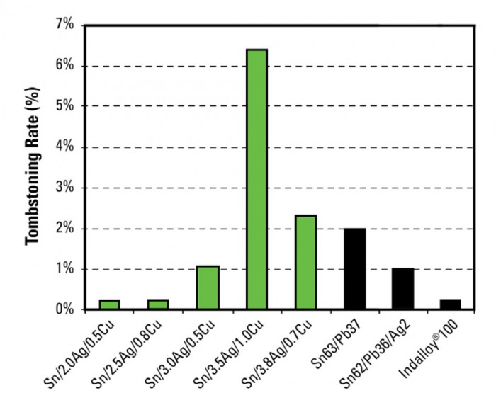
Figure 3: Alloy comparison of tombstoning other than SAC305. The green bars are lead-free alloys; the black are lead-containing alloys
Board Design
It is extremely important for manufacturing engineers to work closely with design engineers to eliminate challenges and defects in PCB manufacturing. Tombstoning is one defect where proper design could eliminate the issue. If the board design has a heat-sink (a copper layer, for example) under or near one side of a passive component, and the other side is further away, the heat-sink could affect the thermal equilibrium of the assembly; the solder paste on the side without the heat-sink could become liquidus first, which could cause a tombstoning defect.
Stencil Design
Minimizing the amount of solder paste printed on the PCB pads will also reduce tombstoning. It is especially helpful to reduce the amount of solder printed directly behind the ends of the passive, which will eliminate nearly all tombstoning forces. A typical stencil design to help achieve this goal is shown in Figure 4. In some experiments, this design completely eliminated tombstoning.
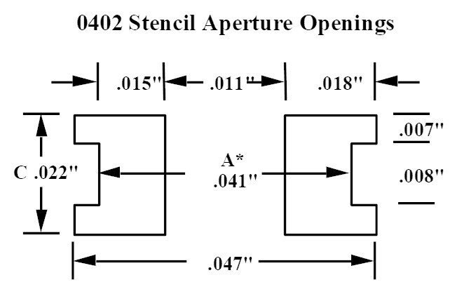
Figure 4: A stencil design to minimize tombstoning in 0402 passives.
Printing
Printing process and transfer efficiency are key components of many end-of-the-line defects, including tombstoning. If one side of a passive component has more solder paste present than the other side, the component might be placed in a position where it is contacting only the higher deposit. This would most likely result in a tombstone defect. The use of Solder Paste Inspection (SPI) equipment can help ensure that solder paste deposits are within specification, and that one deposit is not higher than another. Optimization of the aperture’s size and shape will also help minimize the variation of solder paste volume between pads.
Placement
Placement force and/or improper Z-height can often be the reason why tombstoning occurs. It is important to ensure that placement pressure and Z-height are appropriate for the assembly and optimized prior to production. It is also possible that parts can be skewed when placed. Although solder tends to self-align, components placed incorrectly and out of alignment can result in tombstoning.
Reflow
One approach to minimizing tombstoning is to decrease the total heat input during reflow by gradually increasing the ramp rate; however, this condition might be difficult to achieve in a reflow oven. Another option is to use a soak-type reflow profile to achieve thermal equilibrium between the two solder paste deposits so that both deposits enter the liquidus phase at the same time.
In addition to avoiding solders without a plastic range, a nitrogen atmosphere in the reflow oven tends to exacerbate tombstoning because nitrogen increases the wetting speeds and enables the surface tension forces to appear more rapidly. Unless there are fine-feature solder paste deposits or Package-on-Package (PoP) assemblies on the board, there most likely won’t be a reason to use nitrogen as most top-tier modern solder pastes can perform well in an air reflow atmosphere.
Conclusions
Tombstoning can be minimized by following the guidelines laid out in this article. A reliable way to minimize tombstoning is to use a solder alloy that has a large plastic range, such as Indalloy®100 (leaded) or SAC305 (Pb-free). It is also important to keep an open dialogue with the board designers to minimize heat-sinks near or under one side of the passive components. Use a reflow soldering temperature profile that slowly moves though solidus to liquidus, or minimizes thermal mismatch with a soak. Incorporate SPI to ensure that the solder deposits are similar heights and within specification, and print a solder deposit that is small, especially at the two ends of the passive. Ensure the placement pressure and Z-height are appropriate and the parts are not placed with a skew. Avoid using nitrogen in the reflow oven; with a good solder paste, it is unnecessary and exacerbates tombstoning.
Cheers,
Dr. Ron