
Semiconductor Packaging & Assembly
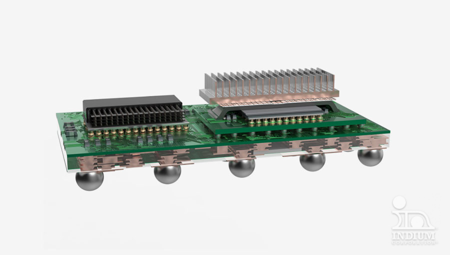
2.5D and 3D Packaging
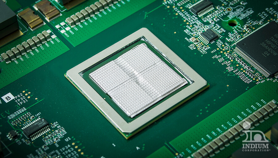
To boost performance, integration, and system capabilities in semiconductor devices, the industry is increasingly adopting 2.5D and 3D packaging. This consolidates multiple integrated circuits (ICs) into a single package, a crucial trend in miniaturization during an era of heterogeneous integration. As a global leader in designing, formulating, manufacturing, and supplying semiconductor-grade fluxes, pastes, and related materials, Indium Corporation is the proven expert for your packaging needs.
Overview
Advancing Semiconductor Integration with the Power of 2.5D and 3D Packaging
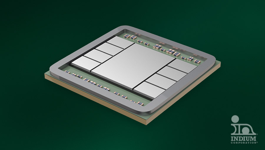
More than Moore, 2.5D and 3D packaging are sophisticated semiconductor integration technologies aimed at enhancing performance and system capabilities. These techniques enable the incorporation of diverse process nodes into a single package. In 2.5D packaging, dies are positioned side by side, while 3D packaging involves stacking the dies vertically. Indium Corporation collaborates with top-tier customers and equipment partners to innovate and refine materials and assembly processes in this rapidly evolving realm.
Benefits
Driving Innovation in Packaging Materials Through Strategic Collaborations
Strategic Partnerships
Leading customers and equipment partners help Indium Corporation develop cutting-edge materials tailored for advanced packaging requirements.
Proven
Process-proven materials are already in use for advanced packaging assembly.
High Yield
Our robust and stable materials achieve the desired yield, especially in challenging packaging assembly processes.
Excellent Technical Service
We provide the support you need to select materials and optimize processes to achieve high-yield.
Related Products
Indium Corporation provides a comprehensive range of materials tailored to meet the demands of 2.5D and 3D packaging solutions.
Flip-Chip Flux
Offers advanced fluxes for flip chip assembly,…
Wafer Bumping Flux
High-quality wafer bumping fluxes for efficient removal…
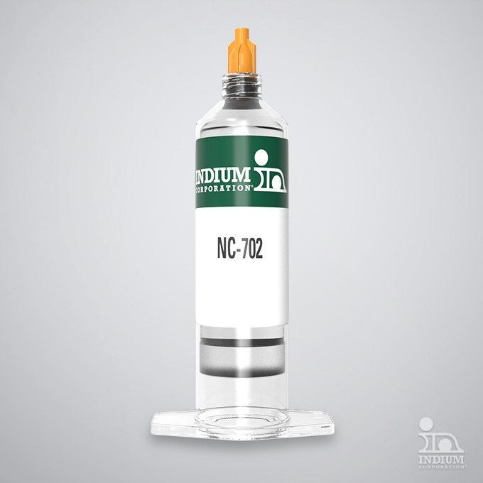
NC-702A for Flip-Chip
Tacking agents supporting no-clean, fluxless reflow for…

Ball-Attach Flux
High-quality water-wash and no-clean ball-attach fluxes.
Thermal Interface Materials
Metal-based TIMs offer low thermal resistance &…
Related Applications
Flip-Chip
A crucial technique in advanced semiconductor packaging.
SiP and Heterogeneous Integration Assembly (HIA)
System-in-package (SiP) and heterogeneous integration solutions
Reflow Soldering with Formic Acid
Flux-free solder pastes and materials for formic…
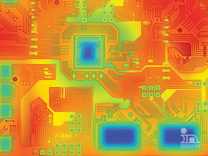
Thermal Management
Thermal solutions for HPC ensuring reliability and…
Related Markets
2.5D and 3D packaging techniques are widely utilized and have a significant impact across industries.


Your Success
is Our Goal
Optimize your processes with the latest materials, technology, and expert application support. It all starts by connecting with our team.