

半導體封裝與組裝
2.5D 與 3D 包裝
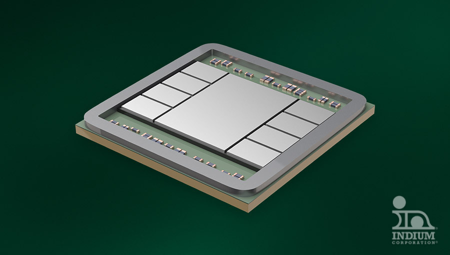
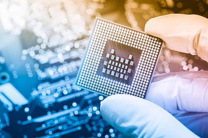
為了提升半導體元件的效能、整合度及系統能力,業界正逐漸採用 2.5D 及 3D 封裝。這將多個積體電路 (IC) 整合到單一封裝中,是異質整合時代小型化的重要趨勢。身為半導體級助焊劑和漿料及相關材料的設計、配方、製造和供應的全球領導者,Indium Corporation 是滿足您封裝需求的可靠專家。
概述
以 2.5D 和 3D 封裝的力量推進半導體整合
比起 Moore,2.5D 和 3D 封裝是精密的半導體整合技術,目的在於提升效能和系統能力。這些技術可將不同的製程節點整合到單一封裝中。在 2.5D 封裝中,晶片是並排放置的,而 3D 封裝則是垂直堆疊晶片。Indium Corporation 與頂尖客戶和設備合作夥伴合作,在這個快速發展的領域中創新和改進材料和組裝製程。
優點
透過策略性合作推動包裝材料的創新

策略夥伴
領先的客戶和設備合作夥伴協助 Indium Corporation 開發專為先進封裝需求量身打造的尖端材料。
證明
經過製程驗證的材料已用於先進的封裝組裝。
高收益
我們堅固穩定的材料可達到理想的良率,特別是在具有挑戰性的包裝組裝製程中。
卓越的技術服務
我們提供您選擇材料和優化製程所需的支援,以達到高產量。
相關產品
Indium Corporation 為滿足 2.5D 與 3D 封裝解決方案的需求,提供量身打造的全方位材料。
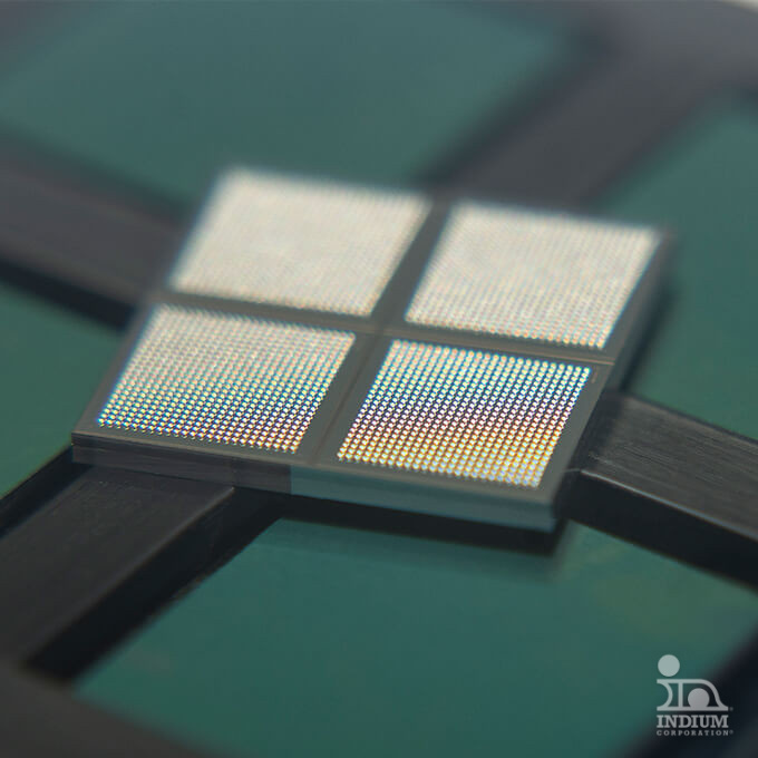
倒裝晶片通量
Offers advanced fluxes for flip chip assembly,…
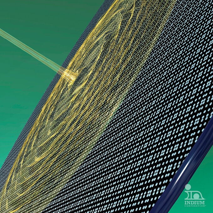
晶圓凸起助焊劑
High-quality wafer bumping fluxes for efficient removal…
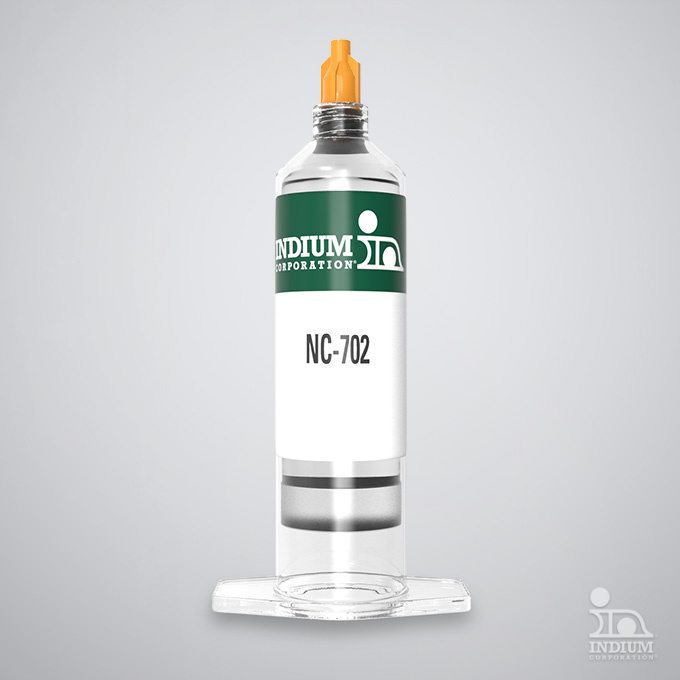
適用於 Flip-Chip 的 NC-702A
Tacking agents supporting no-clean, fluxless reflow for…

球型接頭焊劑
High-quality water-wash and no-clean ball-attach fluxes.
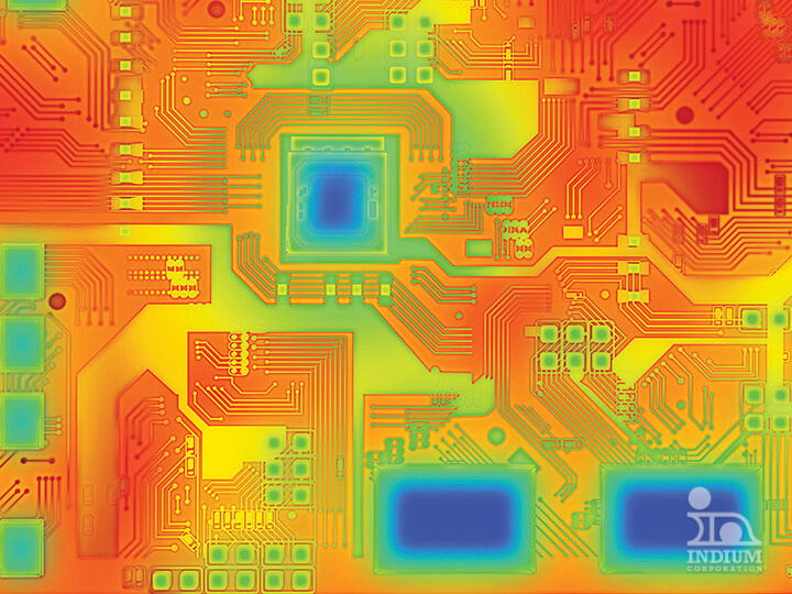
熱介面材料
Metal-based TIMs offer low thermal resistance &…
相關應用程式
倒轉式晶片
一種在先進半導體封裝領域中至關重要的技術。
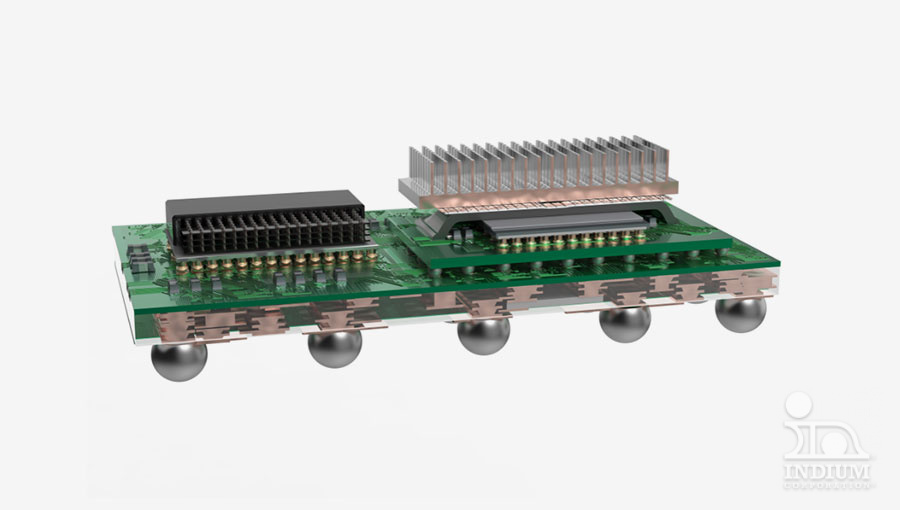
系統級封裝與異質整合組裝技術
系統級封裝 (SiP) 與異質整合解決方案
甲酸回流焊接
Flux-free solder pastes and materials for formic…
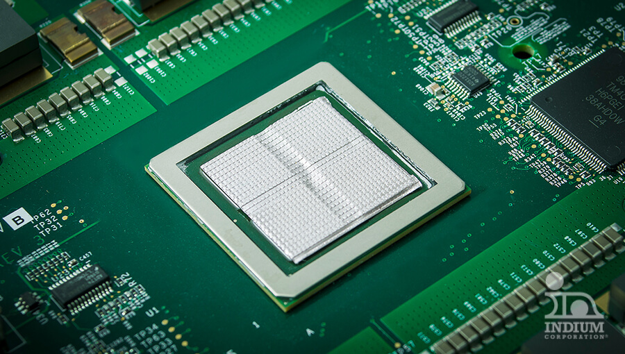
散熱管理
針對 HPC 的散熱解決方案,確保可靠性與……


您的成功
是我們的目標
使用最新的材料、技術和專業應用支援來優化製程。一切從與我們的團隊聯繫開始。