
半导体封装与装配
2.5D 和 3D 包装
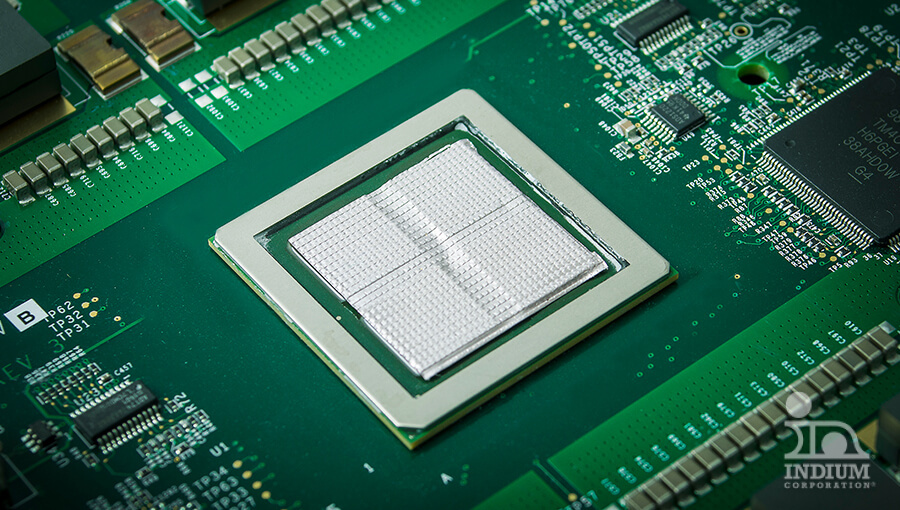
To boost performance, integration, and system capabilities in semiconductor devices, the industry is increasingly adopting 2.5D and 3D packaging. This consolidates multiple integrated circuits (ICs) into a single package, a crucial trend in miniaturization during an era of heterogeneous integration. As a global leader in designing, formulating, manufacturing, and supplying semiconductor-grade fluxes, pastes, and related materials, Indium Corporation is the proven expert for your packaging needs.
概述
利用 2.5D 和 3D 封装技术推进半导体集成
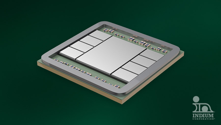
More than Moore, 2.5D and 3D packaging are sophisticated semiconductor integration technologies aimed at enhancing performance and system capabilities. These techniques enable the incorporation of diverse process nodes into a single package. In 2.5D packaging, dies are positioned side by side, while 3D packaging involves stacking the dies vertically. Indium Corporation collaborates with top-tier customers and equipment partners to innovate and refine materials and assembly processes in this rapidly evolving realm.
益处
通过战略合作推动包装材料创新
战略合作伙伴
Leading customers and equipment partners help Indium Corporation develop cutting-edge materials tailored for advanced packaging requirements.
证明
经过工艺验证的材料已用于先进的包装装配。
高收益
我们的材料坚固稳定,可实现理想的产量,特别是在具有挑战性的包装装配工艺中。
卓越的技术服务
我们为您提供选择材料和优化工艺所需的支持,以实现高产。
相关产品
Indium Corporation provides a comprehensive range of materials tailored to meet the demands of 2.5D and 3D packaging solutions.
倒装芯片
提供用于倒装芯片组装的高性能助焊剂……
晶圆成凸
高品质的晶圆成凸 ,可高效去除……
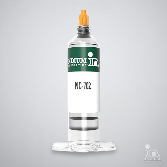
NC-702A for Flip-Chip
Tacking agents supporting no-clean, fluxless reflow for…

植球
高品质的水洗型和免洗 植球 。
热界面材料
Metal-based TIMs offer low thermal resistance &…
相关应用
倒装芯片
A crucial technique in advanced semiconductor packaging.
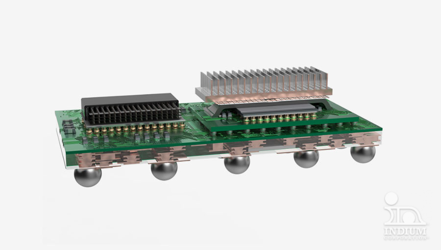
系统级封装(SiP) 异构集成 (HIA)
System-in-package (SiP) and heterogeneous integration solutions
使用甲酸进行回流焊接
Flux-free solder pastes and materials for formic…
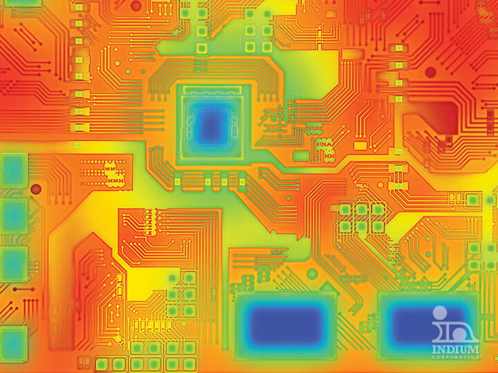
热管理
面向高性能计算(HPC)的散热解决方案,确保可靠性


您的成功
是我们的目标
借助最新的材料、技术以及专家应用 优化您的生产流程。一切都始于与我们团队的联系。