

半导体封装与装配
BGA 连接球
Indium Corporation leads the way in the ball grid array (BGA) ball-attach process, a critical step in semiconductor manufacturing. Our innovative BGA solder flux materials are designed to ensure optimal performance at every stage, from substrate preparation to the most critical ball-attach process. With Indium Corporation, you’re backed by proven solutions that drive superior results.

概述
Enhancing BGA Package Performance with Proven and Innovative Ball-Attach Fluxes
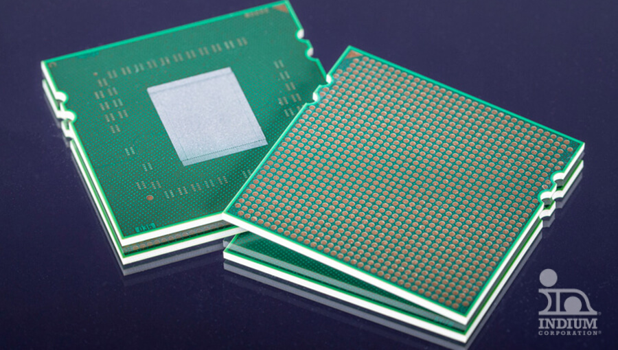
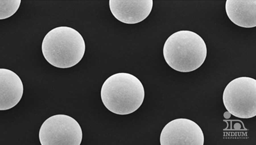
The ball-attach process for BGA packages starts with applying flux, often via pin-transfer from a dipping tray. Next, solder spheres (solder balls) are placed into the flux deposits, followed by reflow of the entire assembly. A reliable ball-attach flux is essential to ensure both the success of this process and the long-term reliability of the final package. Indium Corporation offers high-performance, standard water-soluble ball-attach flux and leads the industry with the first ultra-low residue, no-clean ball-attach flux, onto the flux deposits, specially designed for delicate devices.
益处
Advanced Ball-Attach Flux Solutions for Optimal Performance

Strong Wetting
Ball-attach flux solutions ensure optimal wetting on all metal surfaces, even those with significant contamination or oxidation.
易于清洁
Water-wash flux residue can be effortlessly cleaned post-reflow using pure DI water at room temperature, eliminating the need for chemicals or heated water.
一致性
Consistent flux volume, whether through pin transfer or printing application, is maintained over an extended period of time.
No-Clean
Ultra-low residue ball-attach flux is the perfect choice for sensitive devices that are increasingly difficult to clean sensitive devices.
相关产品
相关应用
焊点/凸块
Achieve robust solder bumps on wafers with…
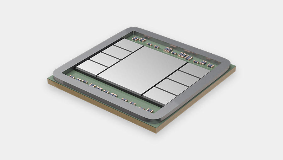
2.5D 和 3D 包装
Techniques to incorporate multiple dies in a…
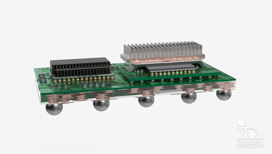
系统级封装(SiP) 异构集成 (HIA)
System-in-package (SiP) and heterogeneous integration solutions


您的成功
是我们的目标
借助最新的材料、技术以及专家应用 优化您的生产流程。一切都始于与我们团队的联系。