

应用
焊点/凸块
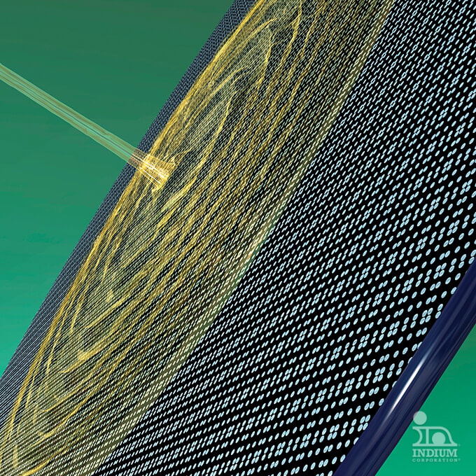
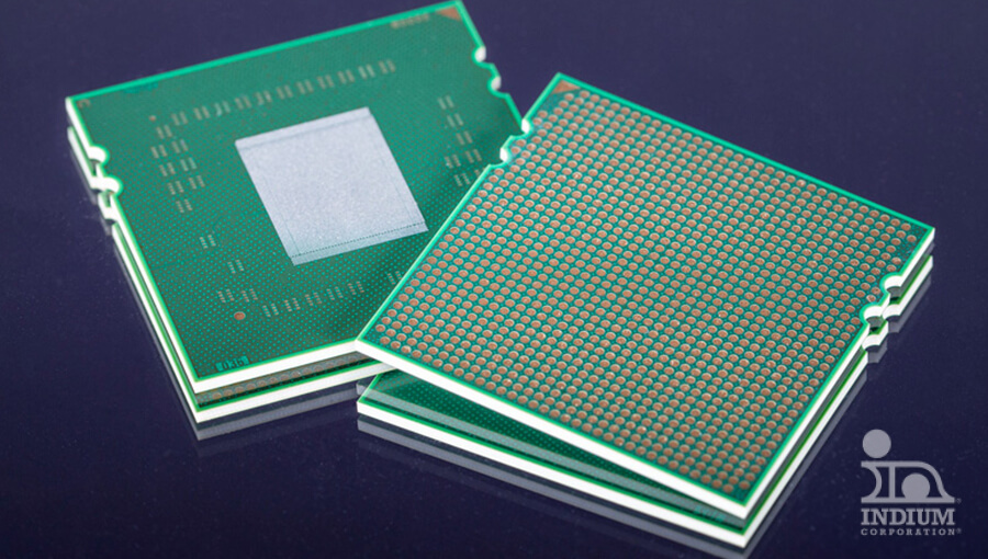
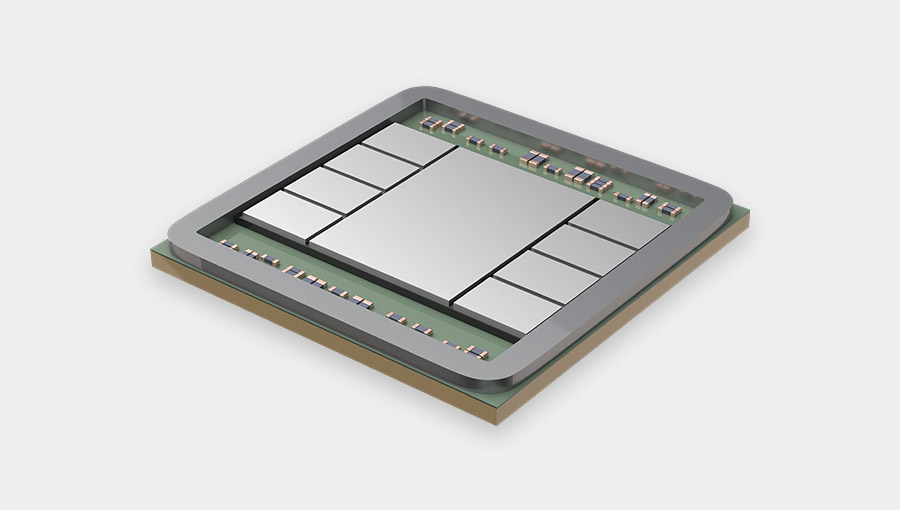
In the semiconductor manufacturing process, bump fusion is crucial for forming solder bumps on wafers, enabling the transfer of electrical signals on semiconductor chips. Indium Corporation’s wafer bumping flux reliably produces flawless, oxide-free solder bumps. With a long-standing reputation for quality, we remain a trusted provider of exceptional wafer bumping flux solutions.
概述
Remove Oxides and Enhance Solderability with Wafer-Bumping Flux
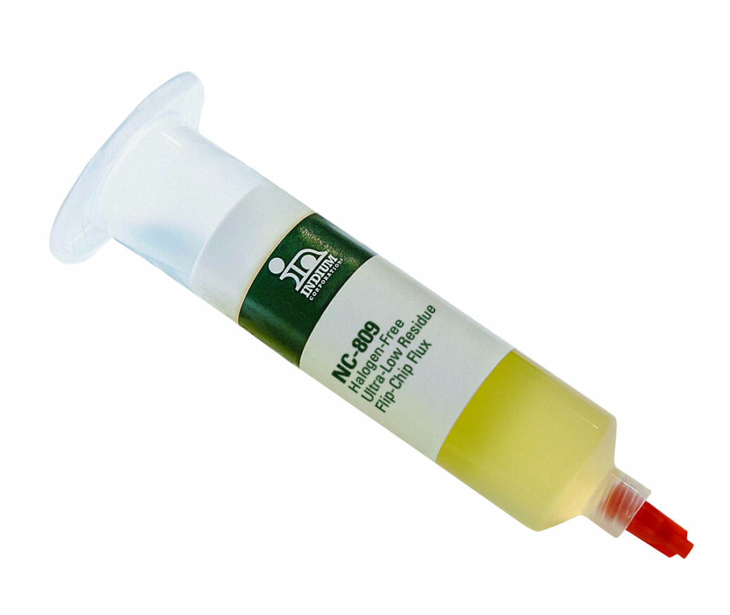
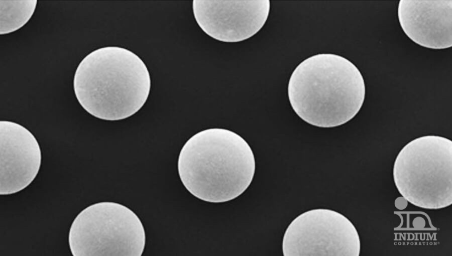
Wafer bumping flux, or bump fusion flux, is low-viscosity material applied via spin-coating onto wafers with solder bumps, copper pillars, or solder-capped surfaces. This specialized flux eliminates oxides and impurities during reflow and cleaning. It transforms irregular, non-spherical, plated, or dented solder bumps on wafers into smooth, oxide-free forms. Available in water-soluble or solvent-based formulations, our wafer bumping fluxes deliver optimal performance by removing oxides, enhancing solderability.
益处
Enhanced Bump Fusion: Cleanable, Versatile, Consistent Solutions
易于清洁
The WS-series can be easily cleaned after reflow with warm DI water, while the SC-series allows for effortless cleaning using widely available industrial solvents or aqueous-based solutions.
广泛的选择
Ideal for a broad range of solder alloy bumps, including lead-free and high lead-containing alloys.
始终如一
Produces smooth, oxide-free solder bumps across various solder alloys, leveraging precision and expertise in the soldering process.
多用途
Can be applied with printing, jetting, dispensing, and spin-coating on 6-inch to 12-inch wafers.
相关应用
植球
Including both water-wash and no-clean ball-attach fluxes

半导体封装和装配
关键的半导体封装确保了功能性和耐久性。
2.5D 和 3D 包装
Techniques to incorporate multiple dies in a…
相关市场
Bump fusion and wafer bumping flux are widely used in markets for wafer-level packaging markets, which demand precise and reliable methods for creating solder bumps on silicon wafers. Wafer bumping flux is particularly essential in the semiconductor packaging and assembly industry, especially for 2.5D and 3D packaging applications. With years of experience in this field, we recognize the critical importance of precision and expertise in the soldering process.


您的成功
是我们的目标
借助最新的材料、技术以及专家应用 优化您的生产流程。一切都始于与我们团队的联系。