
焊料
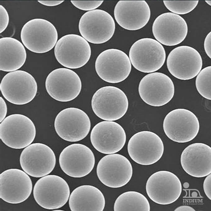
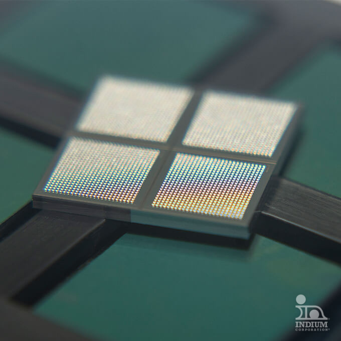
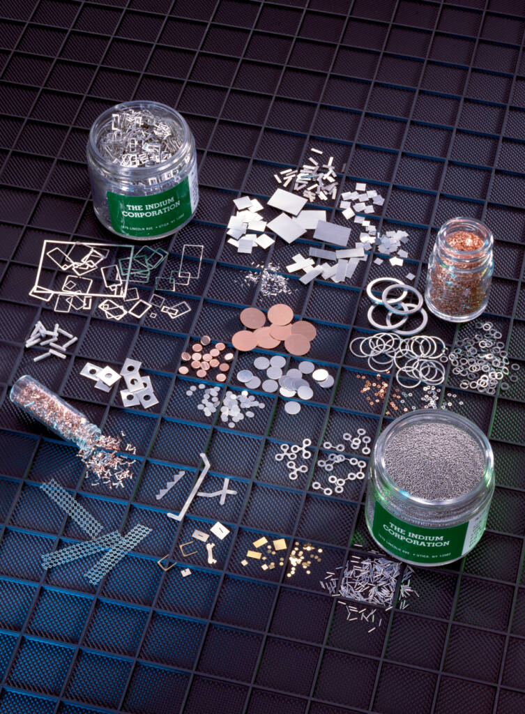
Specialty Solder Spheres
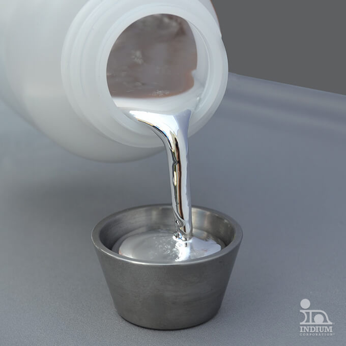
Indium Corporation is a small- to mid-volume supplier of specialty solder spheres. We offer a very wide variety of alloys and size range capabilities from around 0.004″ (100 μm) to 0.063″ (1.6 mm), depending on the alloy. Melting points range from below 90°C to over 700°C.
技术支持:铟泰公司
- Low-Oxide Sphere
- Tight Diameter Tolerance Control
- Tight Alloy Composition Control
概述
功能和优点
Specialty solder spheres are used in a variety of market segments, including medical, transportation and automotive, military and aerospace, high-end mobile, and computing. Clean manufacturing and processing ensure low-oxide levels with no organic contamination. All spheres are manufactured in IATF-16949 certified facilities.
- 精确的直径
- Capable of supplying quantities from 1 sphere to > 20 million per month
- 清洁的生产和加工过程确保了低氧化物含量和无有机物污染
- 白化处理和包装确保清洁的连续性
- 纯金属确保球形成品的高质量
- 在获得 IATF-16949 认证的工厂生产
Solder Sphere Products
Pb-Free Alloys
| Alloy | Indalloy®# | Melting Point Solidus (°C) | Melting Point Liquidus (°C) | Min (in)* | Max (in)* | 最小 (µm)* | 最大 (µm)* |
|---|---|---|---|---|---|---|---|
| In50Sn | 1 | 118 | 125 | 0.004 | 0.030 | 102 | 762 |
| In48Sn (In/Sn eutectic) | 1E | 118 | 0.004 | 0.035 | 102 | 889 | |
| Bi42Sn (Bi/Sn eutectic) | 281 | 138 | 0.008 | 0.109 | 203 | 2,769 | |
| Bi42Sn1Ag | 282 | 139 | 140 | 0.008 | 0.030 | 203 | 762 |
| 99.99In (“Pure Indium”) | 4 | 157 | 0.004 | 0.050 | 102 | 1,270 | |
| Sn20In2.8Ag (Pb-free “Sn63”) | 227 | 175 | 187 | 0.004 | 0.030 | 102 | 762 |
| Sn3.0Ag0.5Cu (SAC305) | 256 | 217 | 220 | 0.004 | 0.065 | 102 | 1,651 |
| Sn4.0Ag0.5Cu (SAC405) | 2562 | 217 | 225 | 0.004 | 0.035 | 102 | 889 |
| Sn4Ag | 121 | 221 | 228 | 0.004 | 0.021 | 102 | 533 |
| Sn5Ag | 132 | 221 | 240 | 0.004 | 0.032 | 102 | 800 |
| 80Au20Sn (Au/Sn eutectic) | 182 | 280 | 0.004 | 0.039 | 102 | 991 |
*Approximate Manufacturable Diameter Range
含铅合金
| Alloy | Indalloy®# | Melting Point Solidus (°C) | Melting Point Liquidus (°C) | Min (in)* | Max (in)* | 最小 (µm)* | 最大 (µm)* |
|---|---|---|---|---|---|---|---|
| Sn46Pb8Bi | 240 | 160 | 173 | 0.010 | 0.030 | 254 | 762 |
| Sn36Pb2Ag (Sn62) | Sn62 | 179 | 181 | 0.004 | 0.030 | 102 | 762 |
| Sn37Pb (63Sn) | 106 | 183 | 0.004 | 0.050 | 102 | 1,270 | |
| Pb25In | 110 | 183 | 192 | 0.004 | 0.027 | 102 | 686 |
| Pb40In | 206 | 197 | 231 | 0.004 | 0.020 | 102 | 508 |
| Pb10Sn | 159 | 275 | 302 | 0.004 | 0.040 | 102 | 1,016 |
*Approximate Manufacturable Diameter Range
产品数据表
Specialty Solder Spheres PDS 97549 R9
相关应用
倒装芯片
A crucial technique in advanced semiconductor packaging.
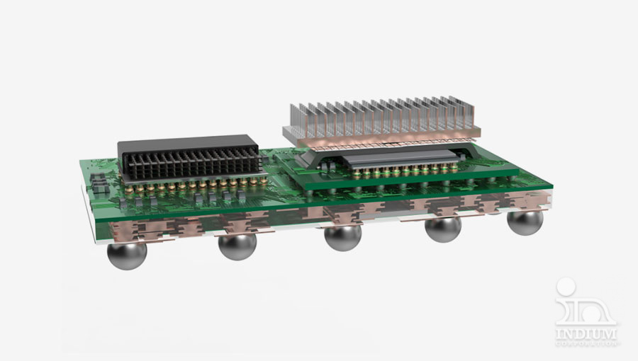
系统级封装(SiP) 异构集成 (HIA)
System-in-package (SiP) and heterogeneous integration solutions
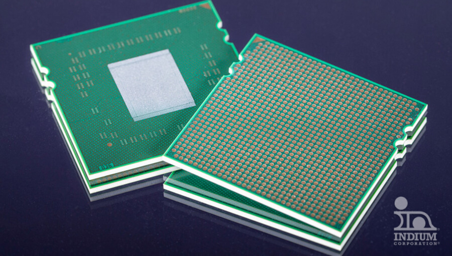
植球
Including both water-wash and no-clean ball-attach fluxes
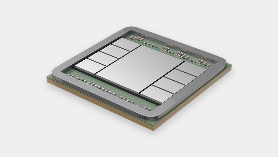
2.5D 和 3D 包装
Techniques to incorporate multiple dies in a…
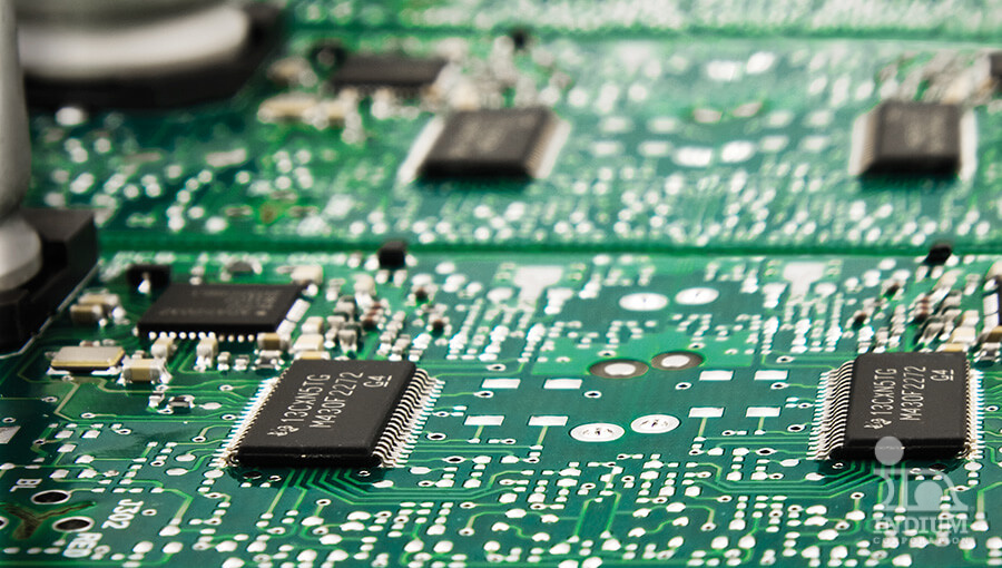
PCB
经过验证且处于行业前沿PCB 组装材料PCB
返修
我们的返修 包括焊锡线、TACflux……


专家支持,结果可靠
您有技术问题或销售咨询吗?我们的专业团队随时为您提供帮助。From One Engineer to Another®不仅是我们的一句口号,更是我们致力于提供卓越服务的承诺。只要您需要,我们随时待命。让我们联系吧!

寻找安全数据表?
您所需的一切——从技术规格到应用 ——都可在此一站式获取。

您的成功
是我们的目标
借助最新的材料、技术以及专家应用 优化您的生产流程。一切都始于与我们团队的联系。