

应用
倒装芯片
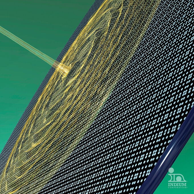
The flip-chip process involves removing individual dies from a wafer mounted on dicing tape, flipping them, and placing them onto a substrate. This substrate can be a printed circuit board, a lead frame, ceramic substrate, or, in the case of 2.5D and 3D assemblies, an interposer or wafer. As a leader in flip-chip flux chemistry, Indium Corporation pioneered the first ultra-low residue, no-clean flip chip flux over a decade ago, setting the standard for the industry.
概述
在日益紧凑的先进封装中实现最高性能
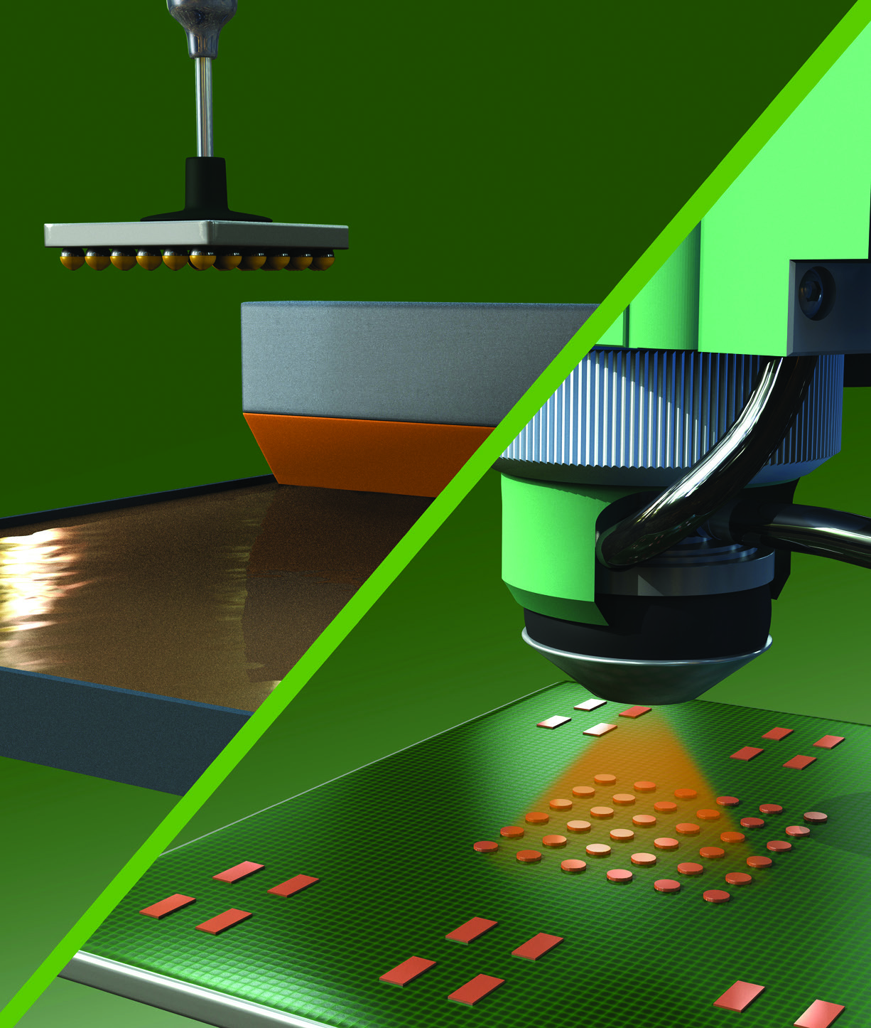
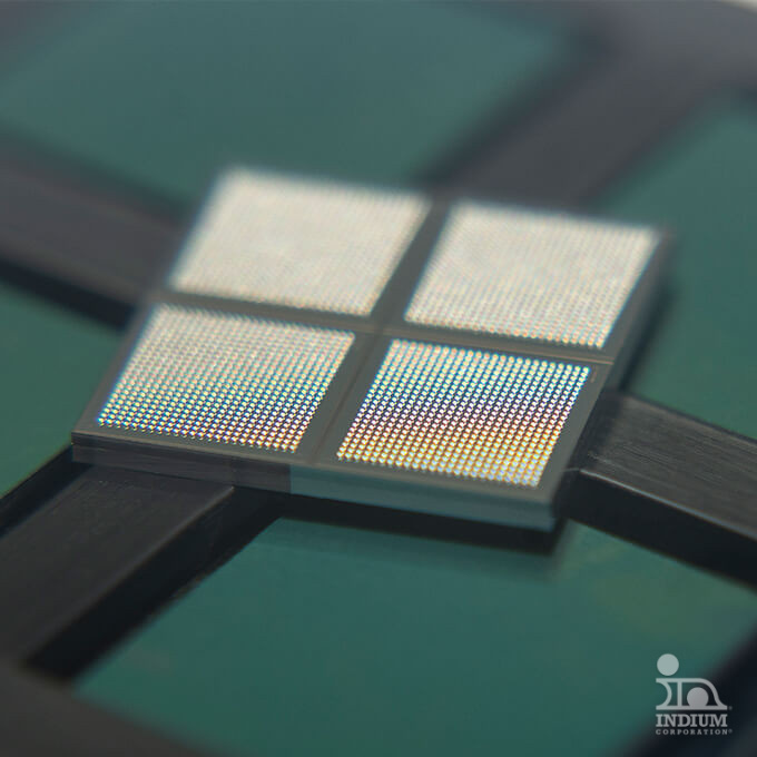
Flip-chip technology is widely used in advanced semiconductor packaging for high performance applications such as microprocessors, GPUs, and RF devices. This process typically involves placing a flipped die dipped with flux onto the substrate, or jetting flux onto the substrate before placing the flipped die, going through mass reflow, or thermos-compression bonding (TCB), or laser-assisted bonding (LAB), to form reliable solder joints for electrical and mechanical connection. This technique eliminates the need for wire-bonding, reducing signal path lengths, thus improving electrical and thermal performance.
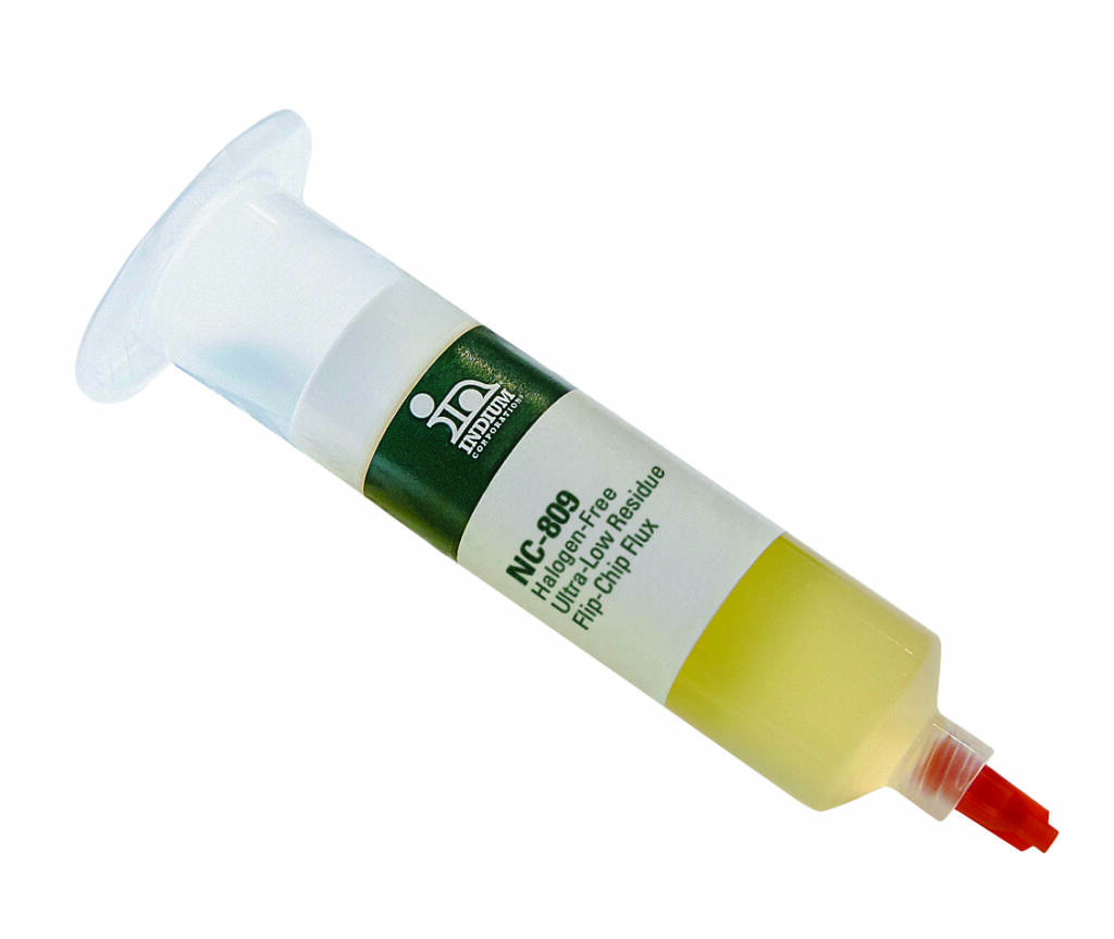
Flip-chip solder bumps have evolved to smaller solder microbumps and copper pillar in recent years, especially for the most advanced semiconductor platform. This shift gives rise to some challenges, such as efficiency in cleaning off flux residue under the tight spacing of flip chip die with high I/O counts, compatibility of flux residue with underfill material, open joints caused by warpage of this and large die, and etc., just to name a few. Our extensive range of flip chip fluxes, are tailored to address some of these challenges, such as ultra-low residue no clean fluxes like NC-809 and NC-26-A, easily cleanable water washable WS-641, and robust water washable WS-446HF.
益处
The Trusted Soldering Material Partner for High-Performance Flip-Chip Assembly

第一
A decade ago, Indium Corporation introduced the first ultra-low residue flux and has since remained a pioneer in the field, offering a diverse range of ultra-low residue fluxes.
一步之遥
Our water-wash formula, WS-446HF, can be use for both ball-attach and flip-chip applications, making it more convenient to use a single flux for both processes.
无通量
Our fluxless tacking agent is designed for the formic acid reflow process in flip chip applications and is qualified for 2.5D applications.
合作伙伴
我们与客户和行业合作伙伴密切合作,为客户量身定制解决方案,满足他们的特定需求。我们经验丰富的技术团队在整个过程中提供咨询和支持,确保每次都能取得成功。
更好的性能
Flip-chip packaging reduces the distance between the chips and the substrate, leading to lower inductance and resistance, which enhances signal integrity and reduces latency.
Improved Thermal Management
The direct connection to the substrate or heat spreader enhances heat dissipation, which is essential for high-performance applications.
更小的占地面积
The flip-chip method enables high-density interconnections and smaller package sizes compared to traditional wire bonding, making it ideal for compact, high-performance devices.
可持续性
这些助焊剂实现了真正的免清洗工艺,通过降低与清洗化学品、水和能源消耗相关的成本,促进了可持续发展。
Flip-Chip Products
相关应用

半导体封装和装配
关键的半导体封装确保了功能性和耐久性。
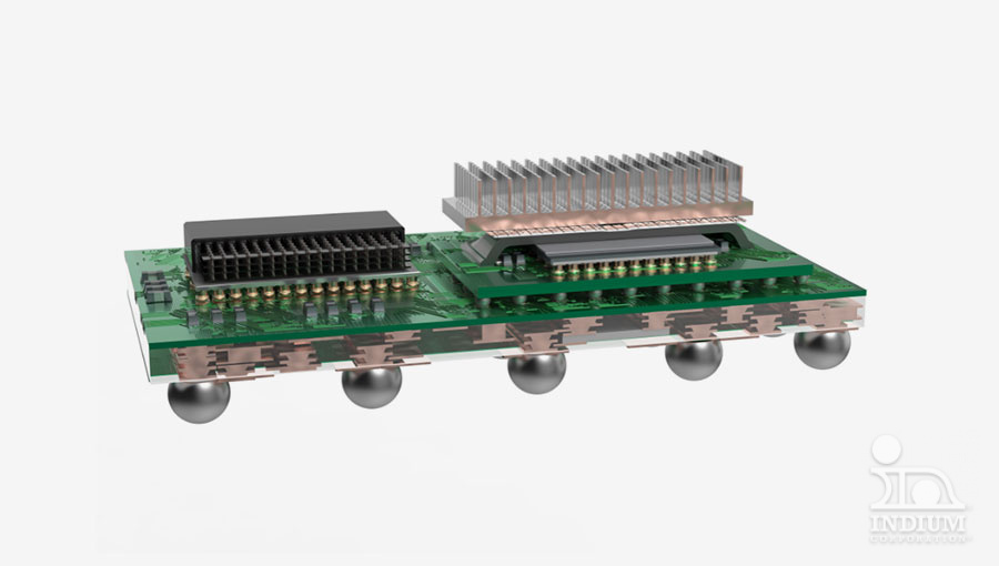
系统级封装(SiP) 异构集成 (HIA)
System-in-package (SiP) and heterogeneous integration solutions


您的成功
是我们的目标
借助最新的材料、技术以及专家应用 优化您的生产流程。一切都始于与我们团队的联系。