
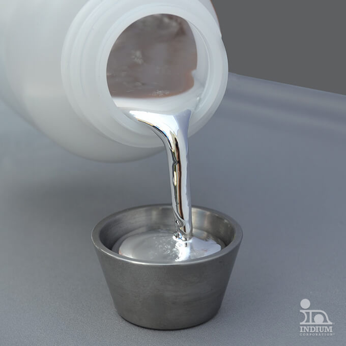
はんだ
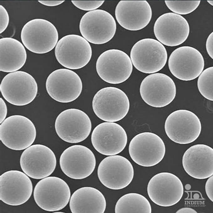
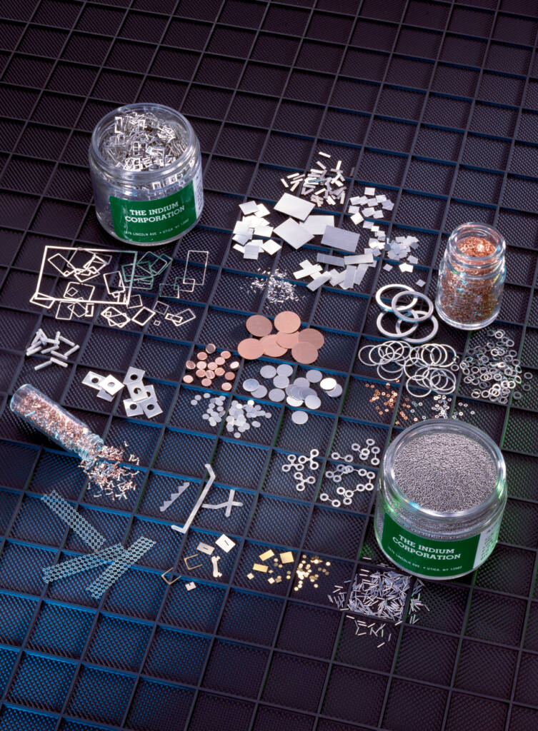
特殊ハンダ球
Indium Corporation is a small- to mid-volume supplier of specialty solder spheres. We offer a very wide variety of alloys and size range capabilities from around 0.004″ (100 μm) to 0.063″ (1.6 mm), depending on the alloy. Melting points range from below 90°C to over 700°C.
Powered by インジウム株式会社
- 低酸化球
- 厳しい直径公差制御
- タイトな合金組成コントロール
概要
特徴と利点
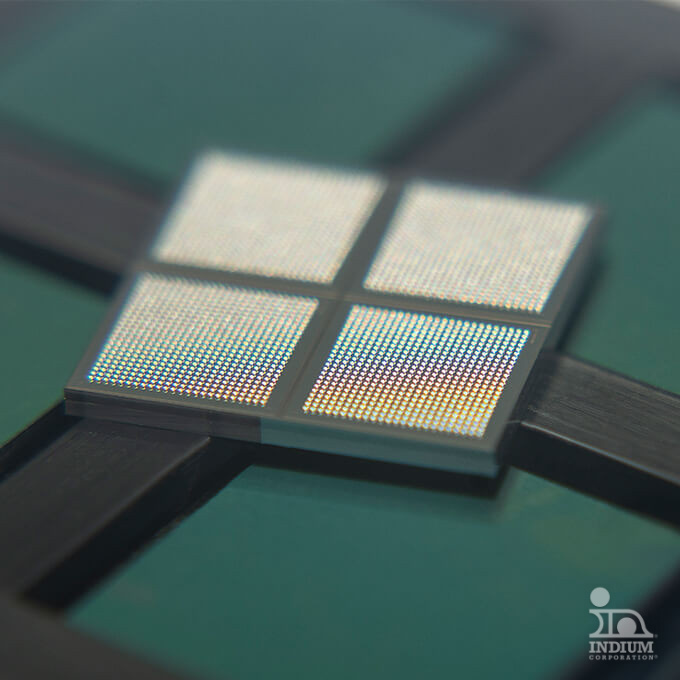
Specialty solder spheres are used in a variety of market segments, including medical, transportation and automotive, military and aerospace, high-end mobile, and computing. Clean manufacturing and processing ensure low-oxide levels with no organic contamination. All spheres are manufactured in IATF-16949 certified facilities.
- 正確な直径
- Capable of supplying quantities from 1 sphere to > 20 million per month
- クリーンな製造・加工により、有機物汚染のない低酸化物レベルを実現
- ホワイトルームの仕上げと包装により、清潔さの持続性を確保
- 純金属が高品質の球体を保証
- IATF-16949認証施設で製造
ソルダースフィア製品
鉛フリー合金
| 合金 | インダロイ | Melting Point Solidus (°C) | Melting Point Liquidus (°C) | Min (in)* | Max (in)* | 最小 (µm)* | 最大 (µm)* |
|---|---|---|---|---|---|---|---|
| In50Sn | 1 | 118 | 125 | 0.004 | 0.030 | 102 | 762 |
| In48Sn (In/Sn eutectic) | 1E | 118 | 0.004 | 0.035 | 102 | 889 | |
| Bi42Sn (Bi/Sn eutectic) | 281 | 138 | 0.008 | 0.109 | 203 | 2,769 | |
| Bi42Sn1Ag | 282 | 139 | 140 | 0.008 | 0.030 | 203 | 762 |
| 99.99In (“Pure Indium”) | 4 | 157 | 0.004 | 0.050 | 102 | 1,270 | |
| Sn20In2.8Ag (Pb-free “Sn63”) | 227 | 175 | 187 | 0.004 | 0.030 | 102 | 762 |
| Sn3.0Ag0.5Cu (SAC305) | 256 | 217 | 220 | 0.004 | 0.065 | 102 | 1,651 |
| Sn4.0Ag0.5Cu (SAC405) | 2562 | 217 | 225 | 0.004 | 0.035 | 102 | 889 |
| Sn4Ag | 121 | 221 | 228 | 0.004 | 0.021 | 102 | 533 |
| Sn5Ag | 132 | 221 | 240 | 0.004 | 0.032 | 102 | 800 |
| 80Au20Sn (Au/Sn eutectic) | 182 | 280 | 0.004 | 0.039 | 102 | 991 |
*おおよその製造可能直径範囲
鉛含有合金
| 合金 | インダロイ | Melting Point Solidus (°C) | Melting Point Liquidus (°C) | Min (in)* | Max (in)* | 最小 (µm)* | 最大 (µm)* |
|---|---|---|---|---|---|---|---|
| Sn46Pb8Bi | 240 | 160 | 173 | 0.010 | 0.030 | 254 | 762 |
| Sn36Pb2Ag (Sn62) | Sn62 | 179 | 181 | 0.004 | 0.030 | 102 | 762 |
| Sn37Pb (63Sn) | 106 | 183 | 0.004 | 0.050 | 102 | 1,270 | |
| Pb25In | 110 | 183 | 192 | 0.004 | 0.027 | 102 | 686 |
| Pb40In | 206 | 197 | 231 | 0.004 | 0.020 | 102 | 508 |
| Pb10Sn | 159 | 275 | 302 | 0.004 | 0.040 | 102 | 1,016 |
*おおよその製造可能直径範囲
製品データシート
Specialty Solder Spheres PDS 97549 R9
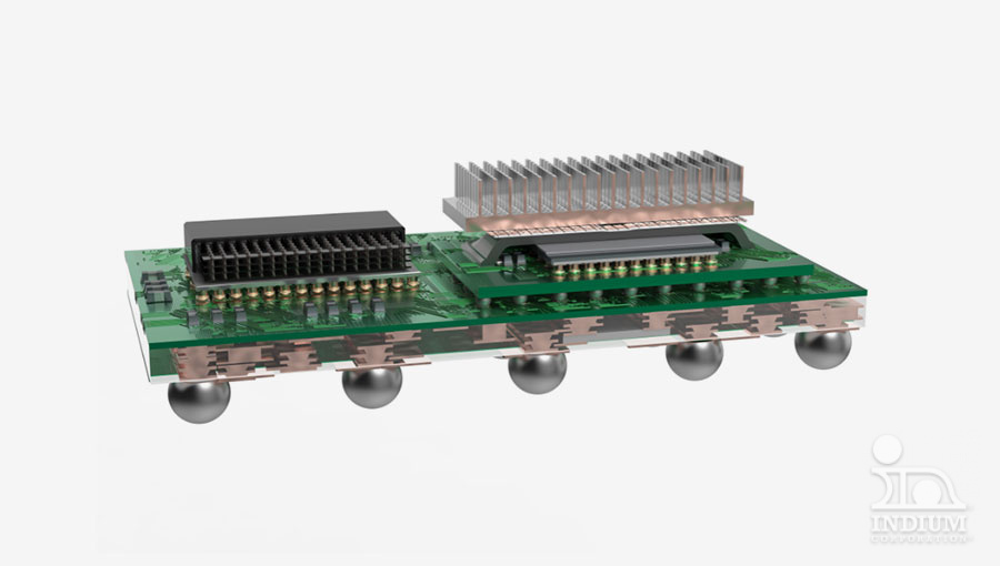
関連アプリケーション
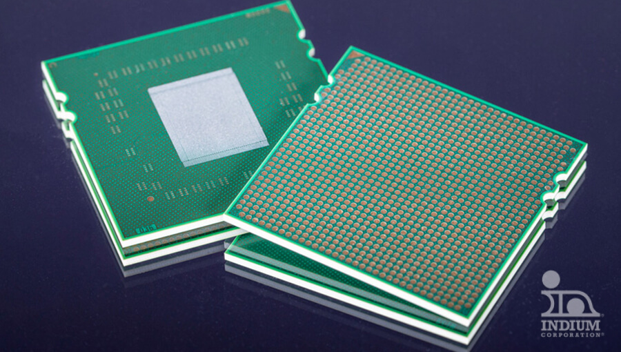
フリップチップ
A crucial technique in advanced semiconductor packaging.
SiPおよびヘテロジニアス統合アセンブリ(HIA)
システム・イン・パッケージ(SiP)と異種統合ソリューション
ボール・アタッチメント
Including both water-wash and no-clean ball-attach fluxes
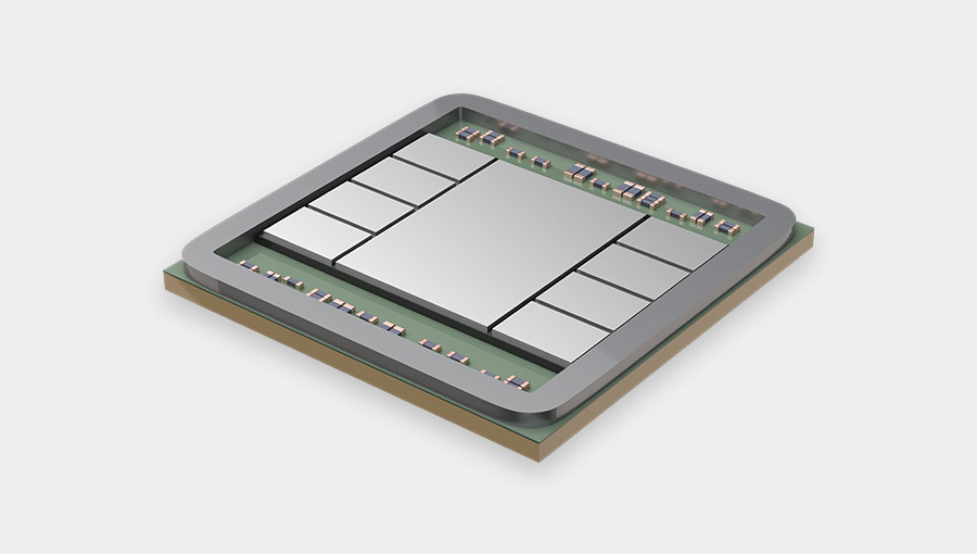
2.5Dおよび3Dパッケージング
Techniques to incorporate multiple dies in a…
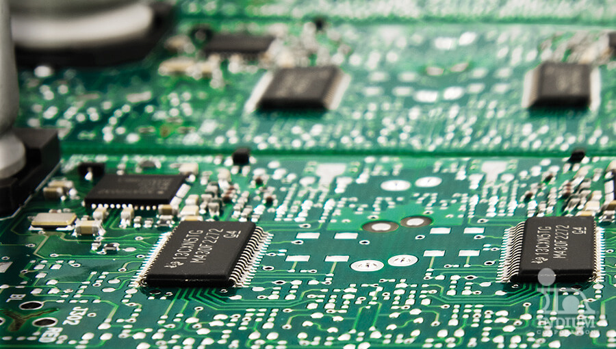
PCBアセンブリ
PCB組立向けの、実績ある最先端の材料…
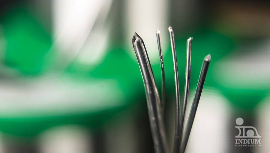
リワーク
Our rework solutions include solder wire, TACflux,…
関連市場


関連商品
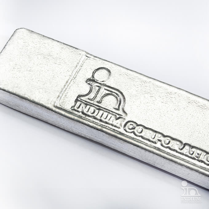
インジウム・インゴット
Purity up to 99.99995%, various Indium Ingot…
液体合金
Explore versatile liquid alloys with low melting…

はんだ合金
融点の異なる幅広い種類のはんだ合金…
はんだプリフォーム
Solder preforms: versatile materials solving sealing &…
専門家による確実なサポート
技術的なご質問や販売に関するお問い合わせはございませんか?当社の専門チームがお手伝いします。「From One Engineer to Another®」は当社のモットーであるだけでなく、卓越したサービスを提供するためのコミットメントでもあります。いつでもご連絡ください。つながりましょう!

安全データシートをお探しですか?
技術仕様からアプリケーションガイダンスまで、必要なものすべてにアクセスできます。

お客様の成功
それが私たちの目標です
最新の素材、技術、専門家によるアプリケーション・サポートにより、お客様のプロセスを最適化します。すべては私たちのチームとつながることから始まります。