
製品紹介
焼結材料
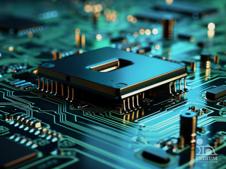
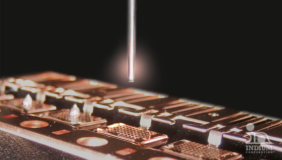
Sintering in electronics assembly, is a bonding technique where high melting temperature metals such as silver or copper are used to form highly reliable interconnects with superior thermal and electrical conductivity. Sintering is a process of steady-state interdiffusion, the metal particles fuse together and fuse with the surfaces being bonded once sufficient heat is applied. Sintering can be performed pressure-less or with applied pressure. Indium Corporation offers both silver and copper sinter pastes for both pressure and pressureless processes.
Powered by インジウム株式会社
- プレッシャーおよびプレッシャーレス処方
- 純粋な焼結材料(エポキシまたはポリマーなし)
- 高金属、低有機物アプローチ
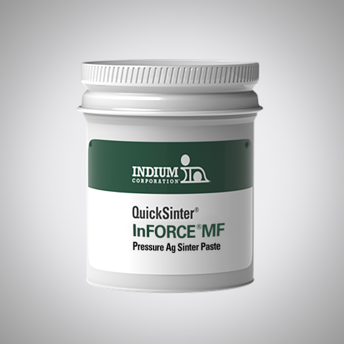
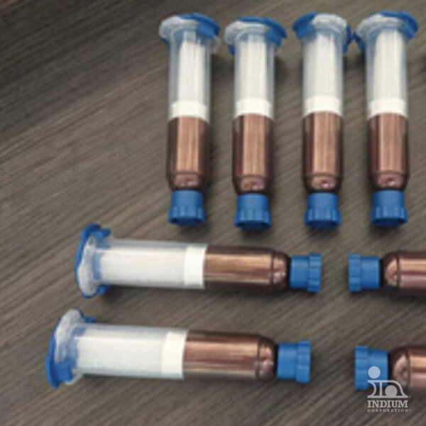
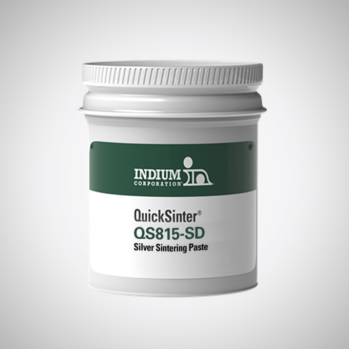
焼結製品
インジウムコーポレーションは、様々な用途に合わせた焼結ペーストを提供しています。InFORCE®シリーズは加圧焼結に最適化されており、InBAKE™シリーズは従来の無加圧焼結に最適です。迅速で小面積の焼結には、QuickSinter®シリーズが卓越した性能を発揮し、迅速で効率的な結果をお約束します。
関連アプリケーション

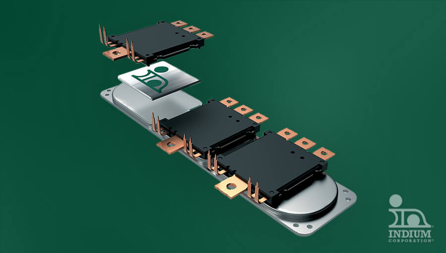
パワーエレクトロニクスのパッケージングとアセンブリ
実績ある高信頼性はんだおよび…の幅広いラインナップ
ダイ・アタッチ
ダイアタッチソリューションには、はんだペーストから金ベースの…
パッケージ・アタッチ
…における課題に対処するための幅広いラインナップ
関連市場
焼結技術や材料は、パワーエレクトロニクス業界のパッケージングやアセンブリ、自動車やe-モビリティなどの市場で広く使用されている。


専門家による確実なサポート
技術的なご質問や販売に関するお問い合わせはございませんか?当社の専門チームがお手伝いします。「From One Engineer to Another®」は当社のモットーであるだけでなく、卓越したサービスを提供するためのコミットメントでもあります。いつでもご連絡ください。つながりましょう!

安全データシートをお探しですか?
技術仕様からアプリケーションガイダンスまで、必要なものすべてにアクセスできます。

お客様の成功
それが私たちの目標です
最新の素材、技術、専門家によるアプリケーション・サポートにより、お客様のプロセスを最適化します。すべては私たちのチームとつながることから始まります。