
アプリケーション
ダイ・アタッチ
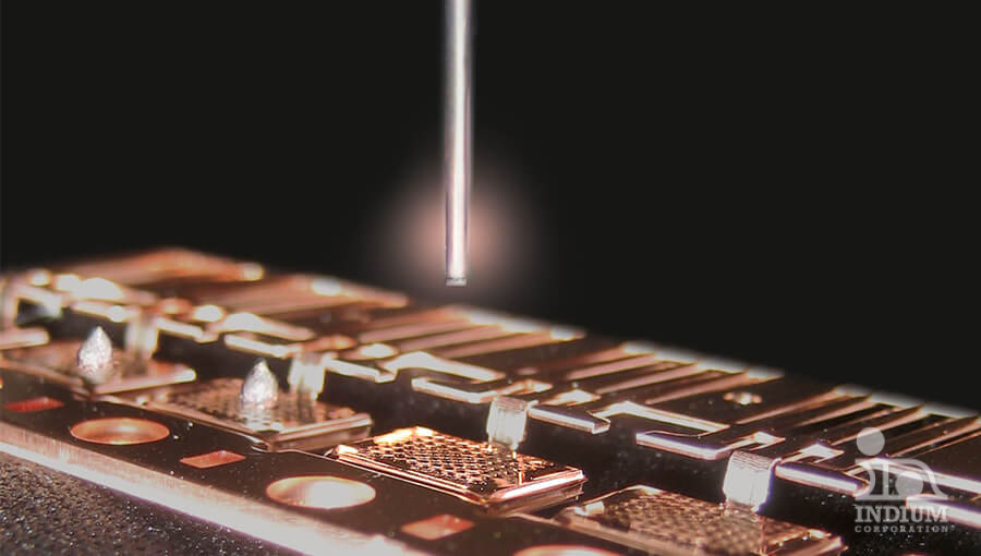
Die-attach involves securing semiconductor dies—typically Si, SiC, GaAs, or GaN—to a lead frame or substrate. This step is essential in establishing a mechanically reliable interconnection while also ensuring that the thermal and electrical properties meet the application’s requirements. Required levels of reliability, thermal conductivity, and electrical conductivity vary across applications, highlighting the importance of selecting the most suitable die-attach material. As a trusted partner in optimizing existing processes and developing innovative solutions, Indium Corporation offers a wide range of die-attach solutions from solder paste, to specialty preforms, to sinter materials.
概要
ハイパワーデバイス用半導体ダイ・アタッチ材料に革命を起こす
IGBTや新興のワイドバンドギャップ半導体などのハイパワーデバイスのダイ・アタッチでは、使用温度、電力密度、信頼性に関する課題が増加しています。従来の高鉛はんだ材料は性能の限界に達しつつありますが、当社は現在および将来の課題を克服するため、先進的な鉛フリー半導体ダイ・アタッチ材料を開発し、技術革新を続けています。
メリット
High Reliability, Thermal Conductivity, and Electrical Conductivity Across Various Applications
低空洞
当社のダイ・アタッチ・ソリューションは、ボイドの低減において卓越した性能を発揮し、アプリケーションに最適な熱性能を保証します。
高信頼性合金
当社では、業界標準を満たす、または上回る、はんだペーストおよびプリフォーム用の信頼性の高い合金を幅広く提供しています。
カスタマイズ
当社は、お客様やパートナーと密接に協力し、お客様固有の要件を満たすダイ・アタッチ・アプリケーション用のオーダーメード・ソルダリング・ソリューションを提供しています。
技術的専門知識
ダイ・アタッチと関連材料に関する深い知識と豊富な経験を持つ当社の技術専門家グローバルチームは、お客様のプロジェクトに貴重なガイダンスとサポートを提供する準備が整っています。
ダイ・アタッチ半導体アプリケーションのための適切な材料の選択
ダイ・アタッチ工程では、高温はんだペーストや金系はんだなど、さまざまな材料から選択することができます。各オプションには明確な利点とトレードオフがあり、特定のアプリケーション要件に基づいて慎重に評価する必要があります。当社では、お客様のニーズに最適な選択ができるよう、実績のあるさまざまな製品とソリューションを提供しています。
金系はんだ
これらの材料は、優れた熱伝導性と電気伝導性が要求される、航空宇宙や軍事などの高コストで信頼性の高い用途に最適です。
焼結
一般的に高性能アプリケーションで使用される焼結は、優れた熱伝導性と電気伝導性を提供し、信頼性と耐久性を向上させるため、パワーエレクトロニクスのWBG半導体に理想的な選択肢となる。
高温ソルダーペースト
ダイ・オン・リードフレーム・アプリケーションで一般的に使用されるはんだダイアタッチは、ダイとリードフレームを機械的に接合すると同時に、熱放散を助けます。ペーストフラックスには、従来のロジン系から超低残渣まで幅広い選択肢があります。合金には、Pbベース、低αPbベース、およびDurafuse®HTのような革新的なPbフリーのソリューションがあります。
プリフォーム
これらの製品は、自動化された製造など、精密な材料管理が必要な用途に適している。また、特注の金型や設計が必要になる場合もあります。当社では、特定の要件に合わせた標準プリフォームとカスタムプリフォームの両方を提供しています。当社の特許技術であるInFORMS®は、ボンドラインの制御と信頼性を高めることで知られており、精度が要求される用途に適しています。
関連商品
インジウムコーポレーションは、多くの選択はんだ付けアプリケーションのニーズを満たすことができるウェーブフラックスのフルラインを提供しています。例えば、WF-9948フラックスは、信頼性とはんだ付け後の残渣を最小限に抑えることが要求される用途に最適です。
高温ソルダーペースト
Pb or Pb-free high-temperature solder pastes.
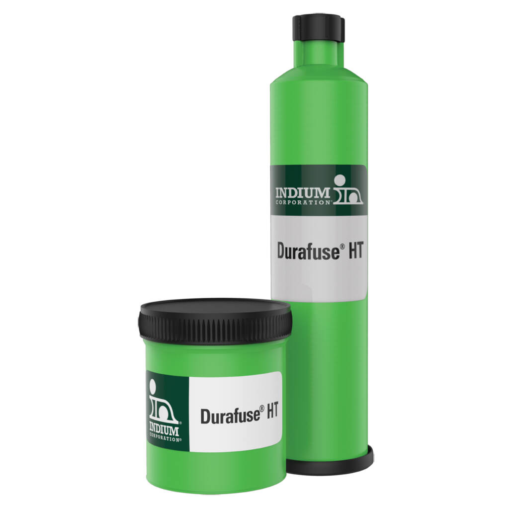
デュラヒューズ・テクノロジー
A patented solder alloy technology to enable…
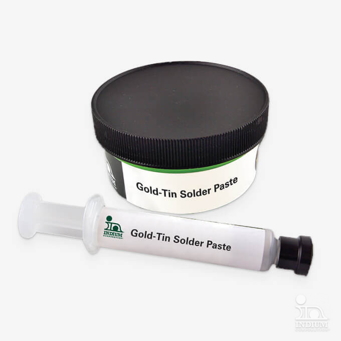
金合金はんだペースト
洗浄不要で水溶性の金・スズ系はんだペースト…

プリフォーム合金
はんだプリフォーム プリフォーム用合金 はんだプリフォームには…
関連アプリケーション

半導体パッケージングおよびアセンブリ
重要な半導体パッケージングは機能性と耐久性を保証する。

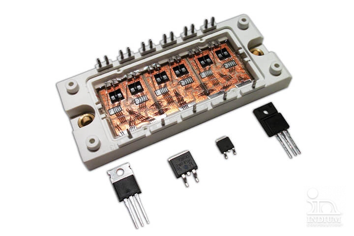
パワーエレクトロニクスのパッケージングとアセンブリ
実績ある高信頼性はんだおよび…の幅広いラインナップ


お客様の成功
それが私たちの目標です
最新の素材、技術、専門家によるアプリケーション・サポートにより、お客様のプロセスを最適化します。すべては私たちのチームとつながることから始まります。