
ソルダーペースト
PCBアセンブリはんだペースト
Indium Corporation produces a wide range of solder paste products to fit every need and challenge in the PCB assembly (PCBA) market space.
Whether you’re dealing with warpage defects, voiding, insufficient paste volume, or reliability issues, our solder pastes are backed by expert support to eliminate issues and deliver high reliability.
Powered by インジウム株式会社
- 幅広いポートフォリオ
- 欠陥をなくす
- 実証された信頼性

製品概要
エラーの最小化
長年のノウハウに裏打ちされたインジウムコーポレーションのPCBAソルダーペーストは、さまざまな用途やニーズに対応し、ボイドや反りによる欠陥などを排除するように設計されています。
幅広いセレクション
当社の広範なポートフォリオには、無洗浄フラックス、水洗フラックス、RMAフラックスに加え、タイプ3からタイプ8までの粉末サイズを持つ多種多様な鉛フリーおよび鉛合金が含まれます。
比類なきサポート
インジウム・コーポレーションは、お客様に卓越した技術サポートを提供し、材料の選択、プロセスの最適化、およびそのガイダンスを支援することをお約束します。
多目的な用途
印刷、ディッピング、ディスペンス、ジェットなど、お客様のプロセスに適したソルダーペーストを提供し、歩留まりを向上させます。
特徴
インジウムコーポレーションは、PCBアセンブリ市場のあらゆるニーズと課題に対応する幅広いソルダーペースト製品を製造しています。

320種類以上のはんだ合金
一般的な合金から特許取得済みの最先端合金技術まで、幅広い選択肢をご用意しています。
Durafuse® Cutting-Edge Alloy Technology
当社の最新の合金技術は、次世代の設計とPCBAアセンブリに力を与えます。
PCBAソルダーペースト製品
無洗浄ソルダーペーストは現代の電子機器製造において最も頻繁に使用されていますが、水溶性ペーストやRMAペーストもユニークな用途に使用されています。当社のソルダーペーストは、Type3からType8まで、数百種類の合金と粉末サイズを取り揃えており、様々な成膜技術の要求に応えられるように設計されています。印刷、ディッピング、ディスペンス、噴流、ピン転写アセンブリーなどの工程を、当社の高品質ソリューションで強化してください。
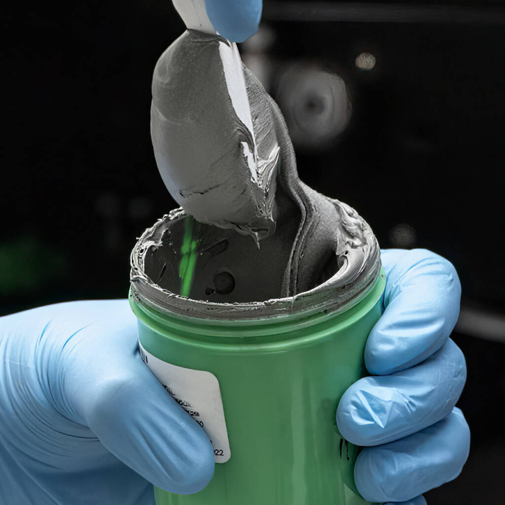
鉛フリーソルダペースト
Utilize a range of Pb-free solder pastes…
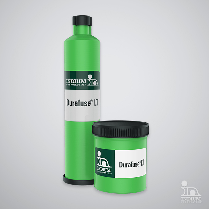
高信頼性ペースト
Wide range of high-reliability solder pastes for…
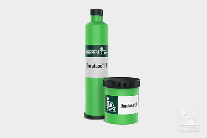
低温ソルダーペースト
幅広い種類の低温はんだペーストを取り揃えています。
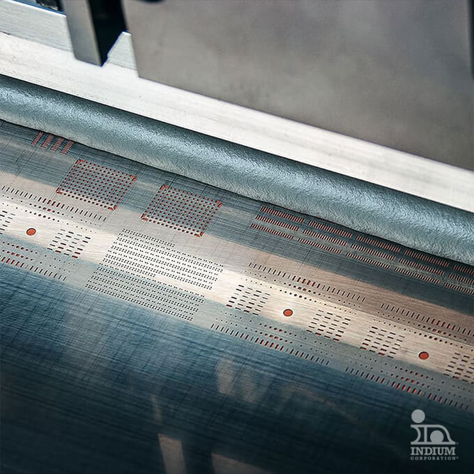
錫-鉛ペースト
Reliable & high-performance no-clean or water-wash tin-lead…
関連アプリケーション
インジウムコーポレーションのPCBアセンブリソルダーペーストは、様々な用途にご利用いただけます。
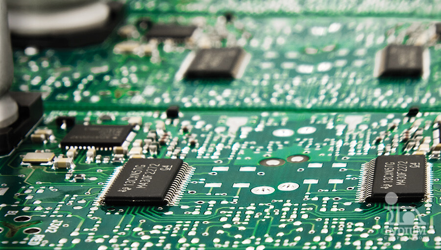
PCBアセンブリ
PCB組立向けの、実績ある最先端の材料…
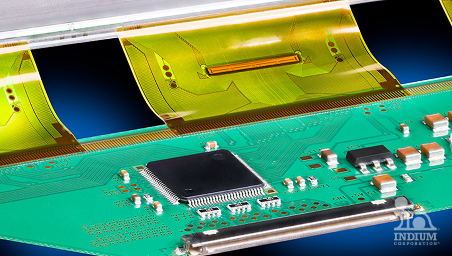
ホットバーはんだ付け
Solder pastes, flux, and more for reliable…
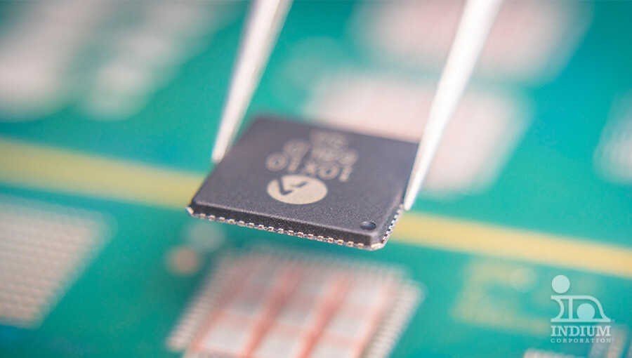
高信頼性
様々な高信頼性PCBAアプリケーションのための様々なオプション。
関連市場
PCBAソルダーペーストは、数多くの産業における電子機器の組み立てに広く使用されています。インジウムコーポレーションのPCBAソルダーペーストは、様々な市場で見つけることができます。


関連商品
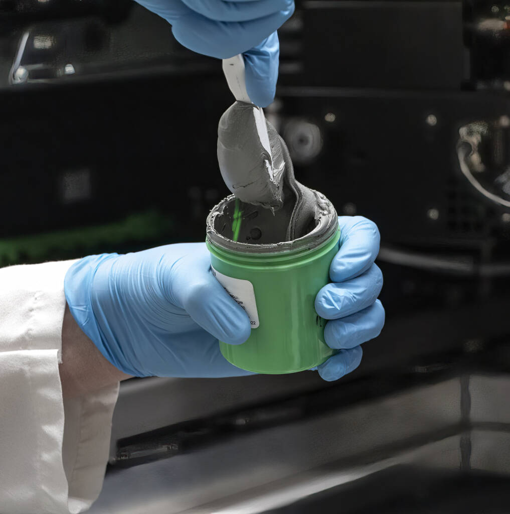
半導体ソルダーペースト
実績のある、幅広い種類の半導体用はんだペースト。
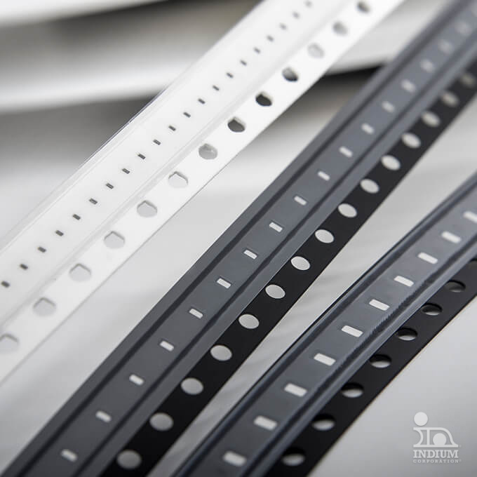
PCBアセンブリ用プリフォーム
信頼性の高いファインピッチを実現する、体積を拡大するプリフォーム…
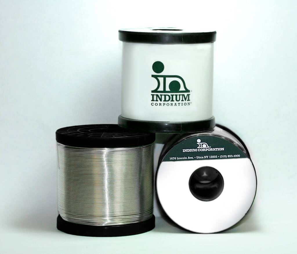
ハンダ線
巻きが均一で、高品質なプレミアムはんだ線…
専門家による確実なサポート
技術的なご質問や販売に関するお問い合わせはございませんか?当社の専門チームがお手伝いします。「From One Engineer to Another®」は当社のモットーであるだけでなく、卓越したサービスを提供するためのコミットメントでもあります。いつでもご連絡ください。つながりましょう!

安全データシートをお探しですか?
技術仕様からアプリケーションガイダンスまで、必要なものすべてにアクセスできます。

お客様の成功
それが私たちの目標です
最新の素材、技術、専門家によるアプリケーション・サポートにより、お客様のプロセスを最適化します。すべては私たちのチームとつながることから始まります。