焼結材料
無加圧焼結
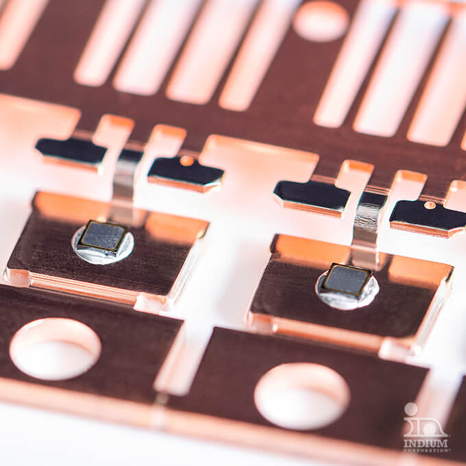
Pressureless sintering is a versatile bonding process used in applications where high conductivity interconnections are critical. Sintered silver or sintered copper bonds offer excellent thermal and electrical conductivity and can withstand high operating temperatures well in excess of 175°C. Pressureless sintering can also be utilized as a Pb-free alternative to traditional die-attach solders. Indium Corporation provides both silver and copper pressureless sinter pastes for a variety of applications.
Powered by インジウム株式会社
- 高金属/低有機物配合
- 銀と銅の焼結オプション
- 低温200℃焼結(Ag)
製品概要
様々な表面仕上げに対応
当社の無圧銀ペーストは銀、金、銅の表面に適合し、銅ペーストは銅、金、ニッケル、銀の表面に適合します。
高温に最適
With melting points of 961°C for Ag and 1,084°C for Cu, sintering is the perfect solution for applications where operating temperatures may exceed 175°C.
鉛フリーダイ・アタッチ・ソリューション
無加圧焼結は、半導体のダイ取り付けにおいて、従来の鉛ベースの高温はんだペーストに代わる鉛フリーの代替品を提供する。
低い処理温度
無加圧焼結は、時間の経過とともに温度の関数として作動する。インジウムコーポレーションのAg焼結ペーストは、200℃という低い温度で処理できます。
無加圧焼結製品
製品データシート
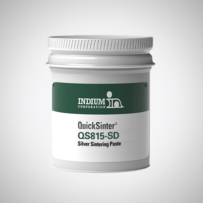
QuickSinter®QS815-AR 無加圧・加圧銀焼結ペースト PDS 99780 R1.pdf
QuickSinter®QS815-SD無加圧銀焼結ペースト PDS 99781 R1.pdf
関連アプリケーション

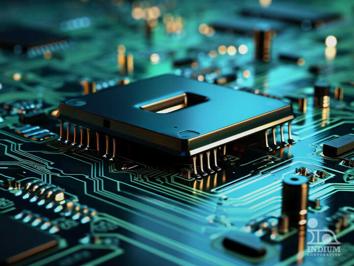
半導体パッケージングおよびアセンブリ
重要な半導体パッケージングは機能性と耐久性を保証する。
パワーエレクトロニクスのパッケージングとアセンブリ
実績ある高信頼性はんだおよび…の幅広いラインナップ

関連商品
専門家による確実なサポート
技術的なご質問や販売に関するお問い合わせはございませんか?当社の専門チームがお手伝いします。「From One Engineer to Another®」は当社のモットーであるだけでなく、卓越したサービスを提供するためのコミットメントでもあります。いつでもご連絡ください。つながりましょう!
安全データシートをお探しですか?
技術仕様からアプリケーションガイダンスまで、必要なものすべてにアクセスできます。

お客様の成功
それが私たちの目標です
最新の素材、技術、専門家によるアプリケーション・サポートにより、お客様のプロセスを最適化します。すべては私たちのチームとつながることから始まります。