
Flussi di semiconduttori
Flusso di bumping per wafer
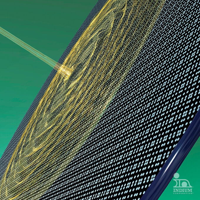
Indium Corporation creates and provides top-tier wafer bumping (bump fusion) fluxes designed to eliminate oxides and other contaminants during reflow and cleaning. Our fluxes can be applied to solder-bumped and copper-pillar/solder-capped wafers through dispensing or spin coating techniques.
Alimentato da Indium Corporation
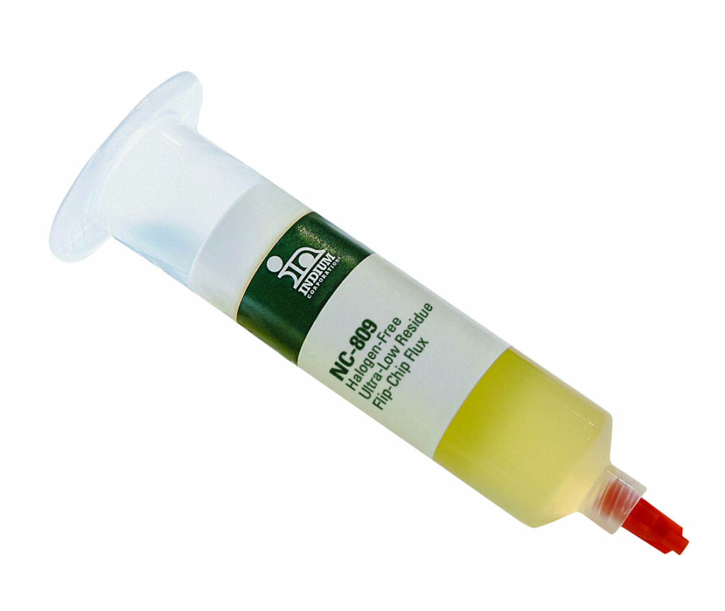
- Water-Washable or Solvent-Cleanable
- Suitable for Use with Various Alloys
- Ampiamente compatibile
Panoramica del prodotto
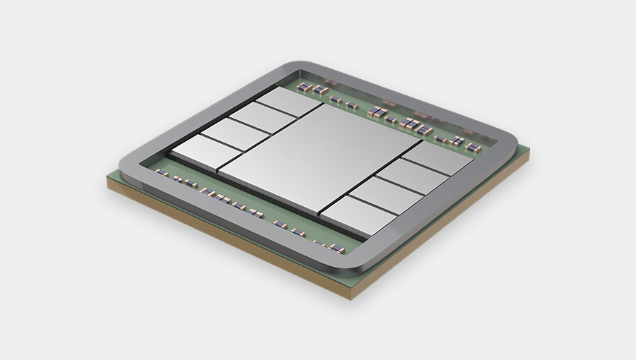
Indium Corporation boasts a longstanding reputation for delivering high-quality wafer-bumping fluxes. Our extensive portfolio features materials tailored for various applications, including traditional wafer bumping processes where fluxes are spin-coated onto plated bumps or copper pillars. Additionally, our products excel in printing applications, where flux is applied to wafers before a ball drop process, commonly used in wafer-level CSP (WLCSP), as well as wafer-level and panel-level fan-out packages.
Our wafer-bumping flux products are compatible with polymers and passivation materials commonly used in wafer processing and packaging assembly.
- Applied by jetting or dispense, followed by spin coating to optimize film thickness
- Reflow in inert atmosphere (typically <20ppm O2 level)
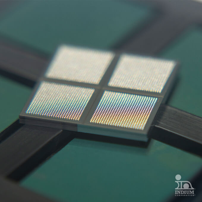
- Converts rough, non-spherical, plated, or wafer probe-dented solder bumps into shiny oxide-free bumps
- Proven applications include copper-pillar microbumps and standard solder bumps
- Applied by printing onto wafer or panel using screen or stencil, followed by a ball drop process
- Wafer bumping flux WS-3401 is used in most advanced 2.5D chip on wafer packaging technology.
- Wafer bumping flux SC-5R has been used for over 10 years in legacy products.
Wafer Bumping Flux Products
Wafer bumping with flux continues to be a widely used method, although some have transitioned to flux-less equipment and processes. Flux is highly effective in producing uniformly low-oxide and well-rounded bumps with optimal morphology.
| Flux Type* | Flux Application Method | Descrizione | Metodo di pulizia | Senza alogeni | Materiale |
|---|---|---|---|---|---|
| SC | Dispence/Spin Coating | High-Pb, SnPb-eutectic, and SnAg solder bumps | Solvent- or aqueous-based chemistry | Sì | SC-5R |
| WS | Dispence/Spin Coating | 20-65 micron pitch copper-pillars with SnAg or Sn100 microbumps | Acqua tiepida DI | Sì | WS-3401 WS-3543 |
| Flux Type* | Flux Application Method | Descrizione | Metodo di pulizia | Senza alogeni | Materiale |
|---|---|---|---|---|---|
| WS | Stampa | 0.5mm and smaller pitch wafer-level or panel-level package; also suitable for LED die-attach application | Acqua tiepida DI | Sì | WS-676 WS-759 WS-829 |
| Considerations | Solder Paste Printing | Plating | Flux/Solder Ball Printing | C4-NP (Suess/IBM) |
|---|---|---|---|---|
| Used In High Volume Manufacturing? | Sì | Sì | Sì | Sì |
| Alloy Restrictions | All solder alloys, as long as powder can be made | Binary alloys only (Sn/Pb, Sn/Ag, Sn/Cu etc.) due to alloy control issues | All solder alloys, as long as sphere can be made | Probably limited to binary alloys |
| Bump Size | Down to around 125micron pitch only. Only 45% of paste volume is metal | Down to 2micron bumps feasible: possibly less | 60micron bump diameter in mass production, but most commonly used for wafer level CSP manufacturing | Unknown |
| Bump Uniformity | OK: can vary significantly with age of solder paste and print process variables | Good | Good with appropriate tight tolerance solderspheres | Good |
| Vuotamento | Common | Little or no with a controlled plating process | Little or no | Little or no |
| Cost Comparison | Low Cost | More Expensive | Low Cost | High Capital Cost |
| Prototyping | Fairly Easy | Complex | Easy | Complex |
Schede tecniche dei prodotti
WS-3401 Flusso per wafer PDS 98197 R4.pdf
WS-3401-A Flusso per wafer PDS 98764 R4.pdf
WS-3518 Flusso per wafer PDS 98431 R3.pdf
WS-3543 Flusso per wafer PDS 98398 R3.pdf
Applicazioni correlate

Confezionamento e assemblaggio dei semiconduttori
Il confezionamento critico dei semiconduttori garantisce funzionalità e durata.
Imballaggio 2.5D e 3D
Tecniche per integrare più matrici in un…
Flip-Chip
Una tecnica fondamentale nel packaging avanzato dei semiconduttori.
Mercati correlati


Prodotti correlati
Flussi di semiconduttori
Ampia gamma di semiconduttori collaudati e di nuova generazione…

Flussante con attacco a sfera
High-quality water-wash and no-clean ball-attach fluxes.
Flusso di flip-chip
Offers advanced fluxes for flip chip assembly,…
Assistenza esperta per risultati affidabili
Avete domande tecniche o richieste di vendita? Il nostro team dedicato è qui per aiutarvi. "Da un ingegnere all'altro®" non è solo il nostro motto: è il nostro impegno a fornire un servizio eccezionale. Siamo pronti quando lo siete voi. Mettiamoci in contatto!

Cercate le schede di sicurezza?
Accedete a tutto ciò che vi serve, dalle specifiche tecniche alle indicazioni per le applicazioni, in un'unica comoda posizione.

Il vostro successo
è il nostro obiettivo
Ottimizzate i vostri processi con i materiali, le tecnologie e l'assistenza applicativa più recenti. Tutto inizia con un contatto con il nostro team.