
半导体助焊剂
晶圆成凸
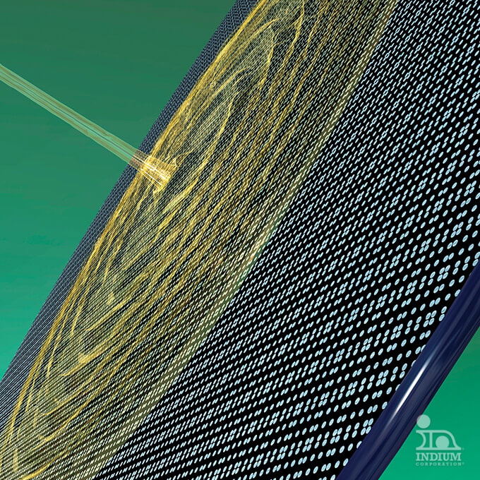
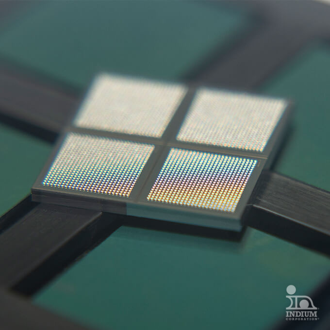
Indium Corporation creates and provides top-tier wafer bumping (bump fusion) fluxes designed to eliminate oxides and other contaminants during reflow and cleaning. Our fluxes can be applied to solder-bumped and copper-pillar/solder-capped wafers through dispensing or spin coating techniques.
技术支持:铟泰公司
- 可水洗或溶剂清洗
- 适用于各种合金
- 广泛兼容
产品概览
Indium Corporation boasts a longstanding reputation for delivering high-quality wafer-bumping fluxes. Our extensive portfolio features materials tailored for various applications, including traditional wafer bumping processes where fluxes are spin-coated onto plated bumps or copper pillars. Additionally, our products excel in printing applications, where flux is applied to wafers before a ball drop process, commonly used in wafer-level CSP (WLCSP), as well as wafer-level and panel-level fan-out packages.
Our wafer-bumping flux products are compatible with polymers and passivation materials commonly used in wafer processing and packaging assembly.
- Applied by jetting or dispense, followed by spin coating to optimize film thickness
- Reflow in inert atmosphere (typically <20ppm O2 level)
- 将粗糙、非球形、电镀或晶片探针凹陷的焊接凸点转化为闪亮的无氧化物凸点
- Proven applications include copper-pillar microbumps and standard solder bumps
- Applied by printing onto wafer or panel using screen or stencil, followed by a ball drop process
- Wafer bumping flux WS-3401 is used in most advanced 2.5D chip on wafer packaging technology.
- Wafer bumping flux SC-5R has been used for over 10 years in legacy products.
Wafer Bumping Flux Products
Wafer bumping with flux continues to be a widely used method, although some have transitioned to flux-less equipment and processes. Flux is highly effective in producing uniformly low-oxide and well-rounded bumps with optimal morphology.
| 助焊剂类型* | Flux Application Method | 说明 | 清洁方法 | Halogen-Free | 材料 |
|---|---|---|---|---|---|
| SC | Dispence/Spin Coating | High-Pb, SnPb-eutectic, and SnAg solder bumps | 溶剂或水基化学 | 是 | SC-5R |
| WS | Dispence/Spin Coating | 20-65 micron pitch copper-pillars with SnAg or Sn100 microbumps | 温 DI 水 | 是 | WS-3401 WS-3543 |
| 助焊剂类型* | Flux Application Method | 说明 | 清洁方法 | Halogen-Free | 材料 |
|---|---|---|---|---|---|
| WS | 印刷 | 0.5mm and smaller pitch wafer-level or panel-level package; also suitable for LED die-attach application | 温 DI 水 | 是 | WS-676 WS-759 WS-829 |
| 考虑因素 | 锡膏 印刷 | 电镀 | 助焊剂/焊剂 球印刷 | C4-NP (苏斯/IBM) |
|---|---|---|---|---|
| 用于大批量生产? | 是 | 是 | 是 | 是 |
| Alloy Restrictions | 所有焊料合金,只要能制成粉末 | Binary alloys only (Sn/Pb, Sn/Ag, Sn/Cu etc.) due to alloy control issues | All solder alloys, as long as sphere can be made | 可能仅限于二元合金 |
| Bump Size | Down to around 125micron pitch only. Only 45% of paste volume is metal | 小至 2 微米的凹凸可行:可能更小 | 60micron bump diameter in mass production, but most commonly used for wafer level CSP manufacturing | 未知 |
| Bump Uniformity | 确定:可能会因焊膏的新旧程度和印刷工艺变量的不同而有很大差异 | 良好 | 使用适当的小公差焊球 | 良好 |
| Voiding | 常见问题 | 电镀过程受控,几乎没有或根本没有 | 很少或没有 | 很少或没有 |
| 成本比较 | 低成本 | 更昂贵 | 低成本 | 高资本成本 |
| 原型设计 | 相当容易 | 复杂 | 简单 | 复杂 |
产品数据表
WS-3401 晶圆助焊剂 PDS 98197 R4.pdf
WS-3401-A 晶圆助焊剂 PDS 98764 R4.pdf
WS-3518 晶圆助焊剂 PDS 98431 R3.pdf
WS-3543 晶圆助焊剂 PDS 98398 R3.pdf
相关应用

半导体封装和装配
关键的半导体封装确保了功能性和耐久性。
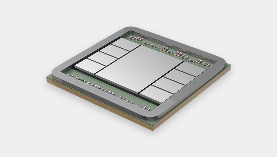
2.5D 和 3D 包装
Techniques to incorporate multiple dies in a…
倒装芯片
A crucial technique in advanced semiconductor packaging.


专家支持,结果可靠
您有技术问题或销售咨询吗?我们的专业团队随时为您提供帮助。From One Engineer to Another®不仅是我们的一句口号,更是我们致力于提供卓越服务的承诺。只要您需要,我们随时待命。让我们联系吧!

寻找安全数据表?
您所需的一切——从技术规格到应用 ——都可在此一站式获取。

您的成功
是我们的目标
借助最新的材料、技术以及专家应用 优化您的生产流程。一切都始于与我们团队的联系。