
Flux de semi-conducteurs
Flux de pompage des plaquettes
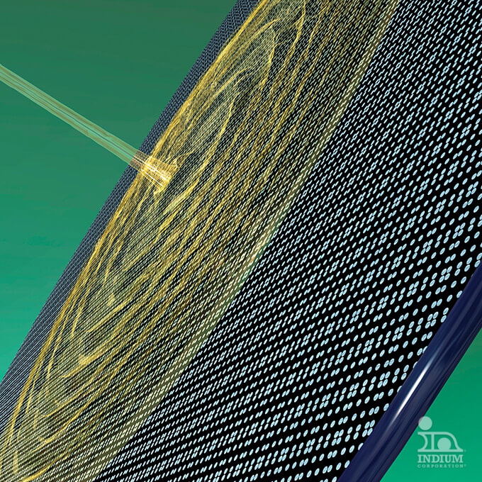
Indium Corporation creates and provides top-tier wafer bumping (bump fusion) fluxes designed to eliminate oxides and other contaminants during reflow and cleaning. Our fluxes can be applied to solder-bumped and copper-pillar/solder-capped wafers through dispensing or spin coating techniques.
Powered by Indium Corporation
- Water-Washable or Solvent-Cleanable
- Suitable for Use with Various Alloys
- Widely Compatible
Aperçu du produit
Indium Corporation boasts a longstanding reputation for delivering high-quality wafer-bumping fluxes. Our extensive portfolio features materials tailored for various applications, including traditional wafer bumping processes where fluxes are spin-coated onto plated bumps or copper pillars. Additionally, our products excel in printing applications, where flux is applied to wafers before a ball drop process, commonly used in wafer-level CSP (WLCSP), as well as wafer-level and panel-level fan-out packages.
Our wafer-bumping flux products are compatible with polymers and passivation materials commonly used in wafer processing and packaging assembly.
- Applied by jetting or dispense, followed by spin coating to optimize film thickness
- Reflow in inert atmosphere (typically <20ppm O2 level)
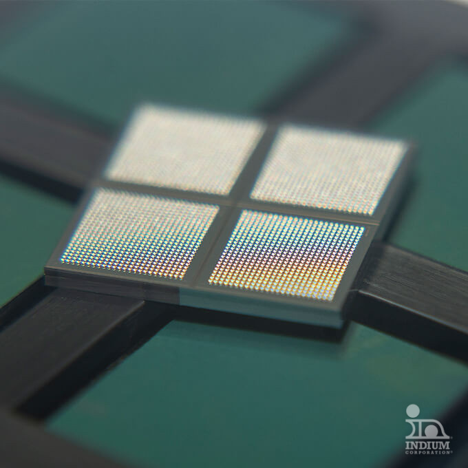
- Converts rough, non-spherical, plated, or wafer probe-dented solder bumps into shiny oxide-free bumps
- Proven applications include copper-pillar microbumps and standard solder bumps
- Applied by printing onto wafer or panel using screen or stencil, followed by a ball drop process
- Wafer bumping flux WS-3401 is used in most advanced 2.5D chip on wafer packaging technology.
- Wafer bumping flux SC-5R has been used for over 10 years in legacy products.
Wafer Bumping Flux Products
Wafer bumping with flux continues to be a widely used method, although some have transitioned to flux-less equipment and processes. Flux is highly effective in producing uniformly low-oxide and well-rounded bumps with optimal morphology.
| Flux Type* | Méthode d'application du flux | Description | Méthode de nettoyage | Sans halogène | Matériau |
|---|---|---|---|---|---|
| SC | Dispence/Spin Coating | High-Pb, SnPb-eutectic, and SnAg solder bumps | Solvent- or aqueous-based chemistry | Oui | SC-5R |
| WS | Dispence/Spin Coating | 20-65 micron pitch copper-pillars with SnAg or Sn100 microbumps | Eau chaude DI | Oui | WS-3401 WS-3543 |
| Flux Type* | Méthode d'application du flux | Description | Méthode de nettoyage | Sans halogène | Matériau |
|---|---|---|---|---|---|
| WS | Impression | 0.5mm and smaller pitch wafer-level or panel-level package; also suitable for LED die-attach application | Eau chaude DI | Oui | WS-676 WS-759 WS-829 |
| Considerations | Solder Paste Printing | Plating | Flux/Solder Ball Printing | C4-NP (Suess/IBM) |
|---|---|---|---|---|
| Used In High Volume Manufacturing? | Oui | Oui | Oui | Oui |
| Alloy Restrictions | All solder alloys, as long as powder can be made | Binary alloys only (Sn/Pb, Sn/Ag, Sn/Cu etc.) due to alloy control issues | All solder alloys, as long as sphere can be made | Probably limited to binary alloys |
| Bump Size | Down to around 125micron pitch only. Only 45% of paste volume is metal | Down to 2micron bumps feasible: possibly less | 60micron bump diameter in mass production, but most commonly used for wafer level CSP manufacturing | Unknown |
| Bump Uniformity | OK: can vary significantly with age of solder paste and print process variables | Good | Good with appropriate tight tolerance solderspheres | Good |
| Voie de garage | Common | Little or no with a controlled plating process | Little or no | Little or no |
| Cost Comparison | Low Cost | More Expensive | Low Cost | High Capital Cost |
| Prototyping | Fairly Easy | Complex | Easy | Complex |
Fiches techniques des produits
WS-3401 Wafer Flux PDS 98197 R4.pdf
WS-3401-A Wafer Flux PDS 98764 R4.pdf
WS-3518 Wafer Flux PDS 98431 R3.pdf
WS-3543 Wafer Flux PDS 98398 R3.pdf
Applications connexes

Emballage et assemblage de semi-conducteurs
Un conditionnement critique des semi-conducteurs garantit leur fonctionnalité et leur durabilité.
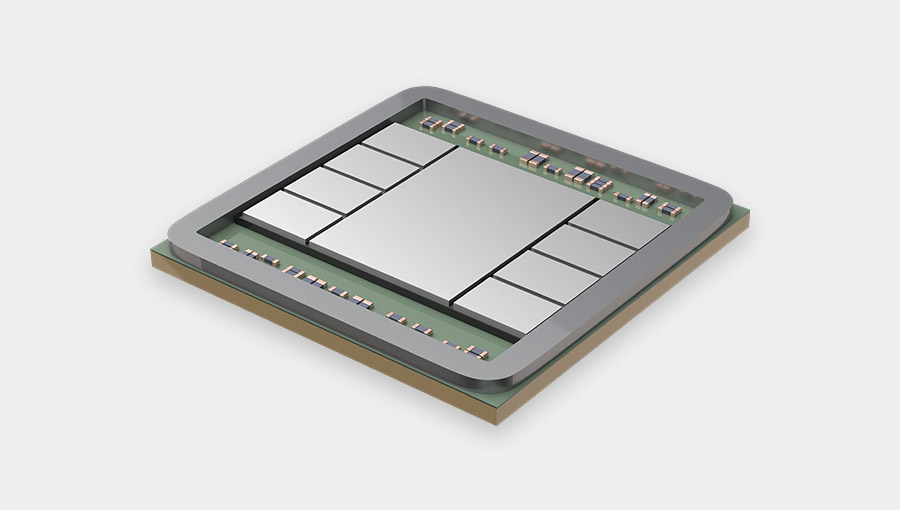
Emballages 2,5D et 3D
Techniques to incorporate multiple dies in a…
Puce
A crucial technique in advanced semiconductor packaging.
Marchés connexes


Produits apparentés
Flux de semi-conducteurs
Extensive portfolio of proven and new semiconductor…

Flux à bille
High-quality water-wash and no-clean ball-attach fluxes.
Flux de la puce
Offers advanced fluxes for flip chip assembly,…
Le soutien d'experts pour des résultats fiables
Vous avez des questions techniques ou commerciales ? Notre équipe dévouée est là pour vous aider. "D'un ingénieur à l'autre®" n'est pas seulement notre devise, c'est notre engagement à fournir un service exceptionnel. Nous sommes prêts quand vous l'êtes. Connectez-vous !

Vous cherchez des fiches de données de sécurité ?
Accédez à tout ce dont vous avez besoin - des spécifications techniques aux conseils d'application - en un seul endroit pratique.

Votre réussite
est notre objectif
Optimisez vos processus grâce aux matériaux et aux technologies les plus récents, ainsi qu'à l'assistance d'experts en matière d'applications. Tout commence par un contact avec notre équipe.