At times, I get questions like, “How long does it take to deposit 20 µm of Indium on my plate using your Indium Sulfamate Bath?” Well, the answer to this question would make it very easy for the customer. Let me show you how to calculate this with ease. In this post, I will derive a simple and easy relation that will work for anyone. Believe me, it’s easy; just use some fundamental relations that we studied in high school. It starts with how many electrons you require to reduce an In3+ ion to an In atom – 3, right!
Alors, quel est le montant de la redevance - 3e !
The time it takes directly depends upon how much charge we’ve got to supply to reduce all those Indium ions, and at what time rate we can supply those – that is “current”!
If you’ve heard of this famous current-charge relation, i =q/t, yes, that is what I am talking about.
Revenons donc à l'essentiel,

If the cathode (where the indium is electrodeposited) is not 100%efficient, it will take a little longer. Let’s say, σ be the efficiency. Then it will take, 1/σtimes longer. For example, if it is50% efficient, it will take, 1/0.5 = 2times longer. So, incorporating efficiency, the equation for time becomes:

Si l'on introduit toutes ces valeurs dans l'équation ci-dessus, on obtient :

Okay, so the answer is, the estimated time to deposit 20µm is 34 minutes, and you know what factors can change this.
And here’s an easy formula to calculate time in minutes for the most widely used units of thickness and current density:

D'accord, pourquoi ne pas appeler ce numéro 30.676 "Shital's Inplate constant" !
Indium Sulfamate Bath from Indium Corporation has a cathodic efficiency of 90%. More efficiency means less time! The typical current density to work on is around 10-20mA/cm2but it can be increased up to100 mA/cm2, maintaining the bath temperature at 20-25°C. Increasing the current density from 20mA/cm2to100 mA/cm2can reduce the deposition time by a factor of 5, i.e. the same 20µm will now deposit in 7 minutes.
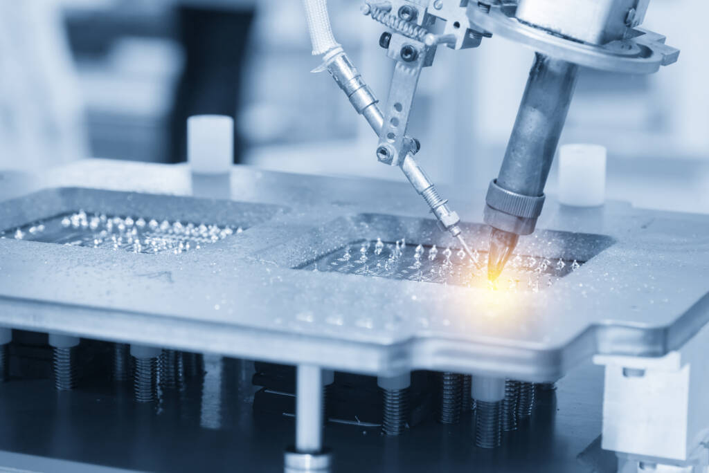
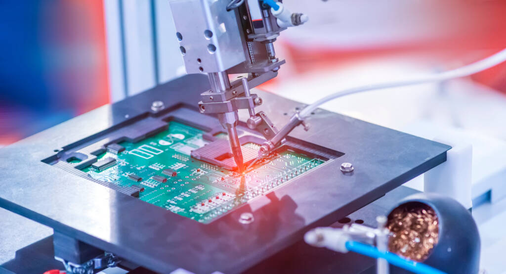
The extensive use of indium plating today dates back to the 1930s when the founders of Indium Corporation developed a commercial indium plating bath for the first time. Recent developments in semiconductor technology and flip-chip bonding utilize indium to create interconnects between layers of wafers. Indium is electroplated onto wafer substrates to create high-density, low-pitch and high-aspect ratio indium bumps. The softness, ductility and wettability of indium ensure a strong and reliable connection between two surfaces, even if they are not perfectly flat or aligned. Furthermore, Indium exhibits stability even at temperatures approaching zero, making it highly suitable for use in semiconductor applications that operate in extreme environments, such as those encountered in space.
Si vous envisagez des projets de galvanoplastie à petite échelle, y compris la restauration et la réparation d'objets métalliques anciens avec une couche d'indium, vous pouvez commencer avec un kit de galvanoplastie sain et facile à utiliser comme celui proposé ici.
Veuillez consulter les documents suivants pour en savoir plus sur l'électrodéposition de l'indium, le bain de sulfamate d'indium et l'électrodéposition des bosses d'indium.
- Obtention d'une structure de grain plus fine grâce au bain de sulfamate d'indium
- Indium Bump Electroplating
- Le placage, une méthode alternative d'application de l'indium
- Préparation correcte de la surface pour le placage à l'indium
- Placage de prototypes à l'aide d'un bain de placage au sulfamate d'indium
- Récupération et élimination de la solution de bain de placage au sulfamate d'indium
For any other inquiries, please contact me.