

Applications
Semiconductor Packaging and Assembly
As semiconductor packaging technologies evolve to meet industry demands of smaller, faster, higher power, more reliable, more efficient devices, packaging and assembly materials play a crucial role. From industry leading die attach solder pastes, ultra-fine solder pastes for SiP, to innovative flux technology for flip-chip bonding and BGA ball attach. Indium Corporation’s semiconductor packaging and assembly materials address todays challenges and help power the future.

Overview
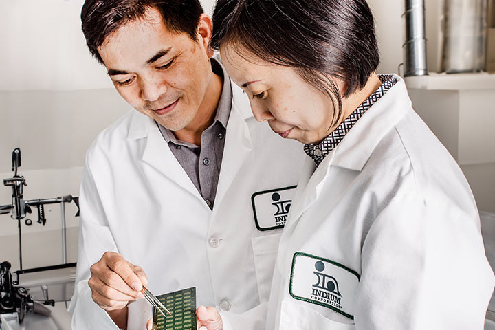
Semiconductor packaging and assembly are critical to manufacturing semiconductor devices, ensuring functionality, efficiency, and reliability. This back-end-of-line (BEOL) process involves encapsulating the silicon die or integrated circuit (IC) to ensure reliable electrical connections to the PCB and other systems. It’s essential for maintaining functionality and durability in diverse environments. Indium Corporation’s expertise in these processes and product selection meets the unique needs of the industry.
Benefits

Proven Materials
Indium Corporation’s advanced products have been integral in the advancement of semiconductor assembly. Our wafer bumping flux WS-3401 and flip-chip flux WS-641 are widely used in 2.5D and advanced semiconductor assembly.
Leading the Way
Over a decade ago, Indium Corporation introduced the first ultra-low residue flux and has remained a pioneer in the field, offering a diverse range of ultra-low residue fluxes.
SiPaste®3.2HF
For over a decade, true washable SiPaste®3.2HF has been the preferred choice for millions of SiP modules.
Fluxless
Through collaboration with industry leaders, we have developed a fluxless adhesive solution for advanced flip chip attachment.
20 Years
With over 20 years of proven performance, our SMQ75 high-temperature high Pb paste remains the industry standard for die-attach on leadframe applications.
High-temperature Pb-free
We’re proud to introduce Durafuse® HT, a drop-in Pb-free solution for replacing Pb-containing solders in high-temperature applications.
5 Billion
To date, over 5 billion front-end SiP modules have been manufactured using Indium Corporation’s semiconductor materials, with continuous growth expected.

Sustainability
These fluxes enable a true no-clean process, driving sustainability by reducing costs related to cleaning chemicals, water, and energy consumption.
Essential Considerations in Semiconductor Packaging & Assembly
Semiconductor assembly involves the process of packaging and interconnecting semiconductor chips or integrated circuits onto a substrate to create functional electronic devices. Semiconductor packaging involves these key considerations:

Interconnect Reliability
Ensuring robust electrical connections to minimize signal loss and resistance.
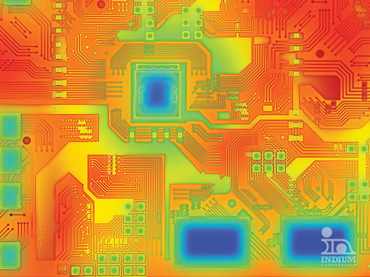
Thermal Management
Implementing efficient heat dissipation solutions to prevent overheating and maintain device performance.
Material Compatability
Selecting packaging materials with compatible coefficients of thermal expansion (CTE) to reduce stress on interconnects and prevent mechanical failures due to thermal cycling.
Semiconductor Packaging & Assembly Products
Indium Corporation offers a full line of wave fluxes that can meet the needs of numerous selective soldering applications. For example, the WF-9948 flux is excellent for those applications where reliability and minimal post-soldering residues are required.
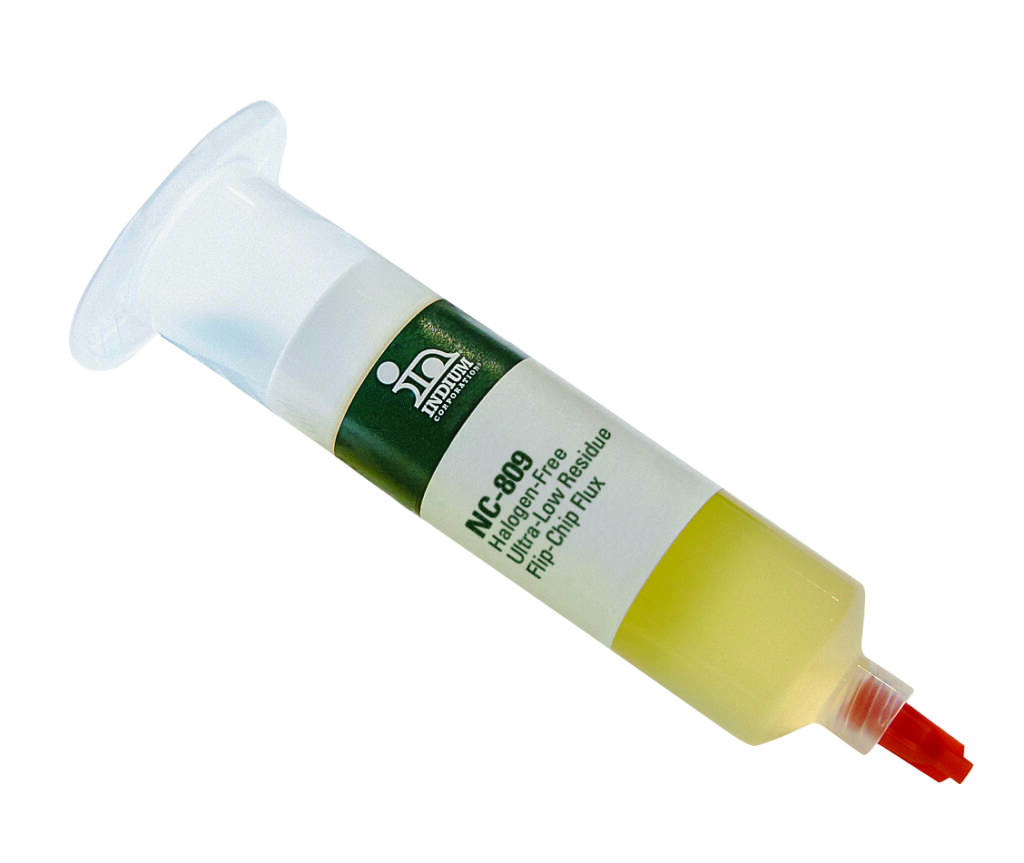
Semiconductor Fluxes
Extensive portfolio of proven and new semiconductor…
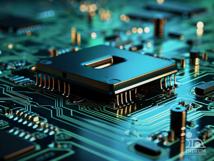
Sintering Materials
Pressure or pressureless silver or copper sinter…
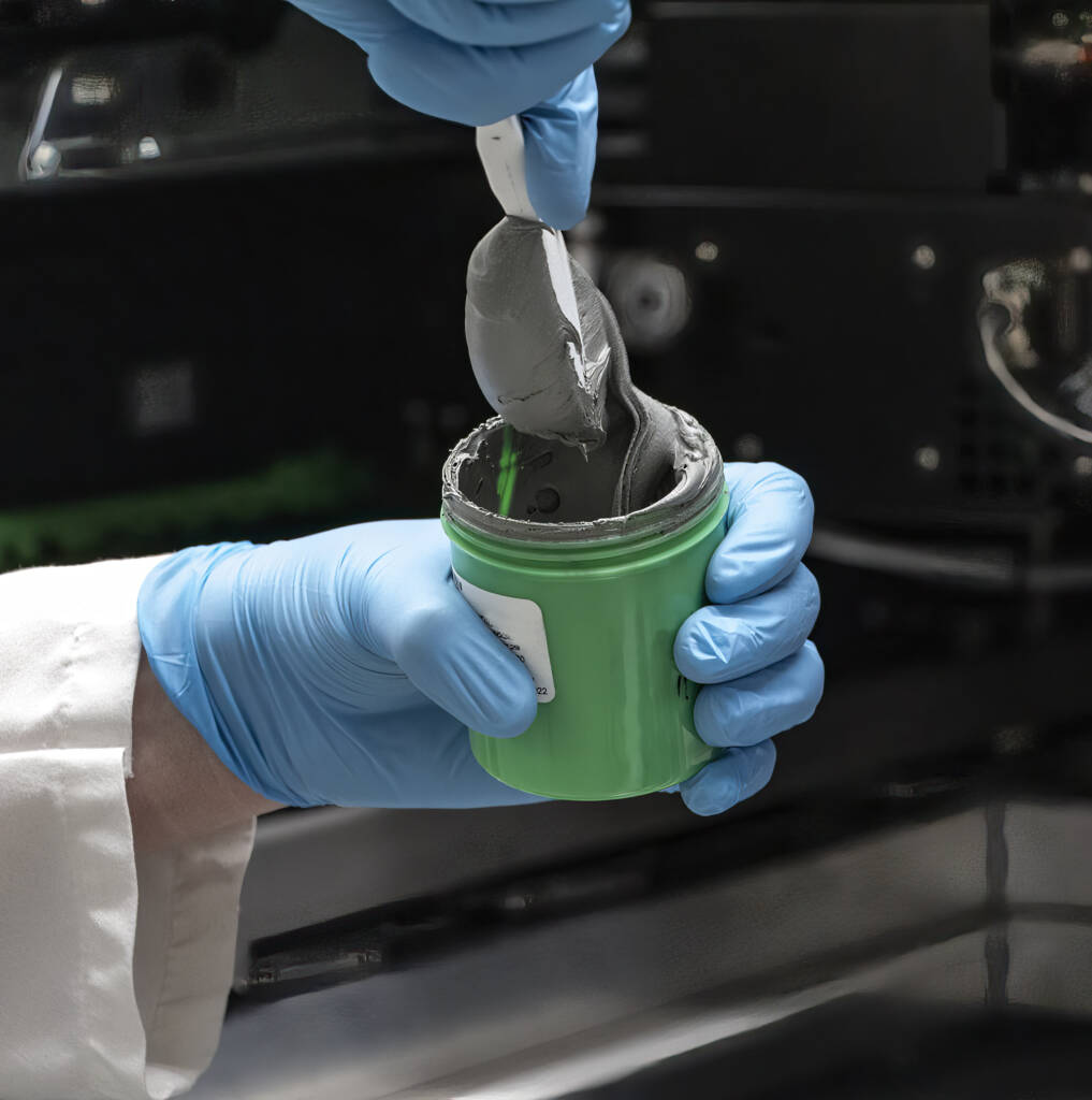
Semiconductor Solder Pastes
Proven diverse range of semiconductor solder pastes.
Thermal Interface Materials
Metal-based TIMs offer low thermal resistance &…


Your Success
is Our Goal
Optimize your processes with the latest materials, technology, and expert application support. It all starts by connecting with our team.