Thermal managementis becoming an ever more critical challenge for semiconductor devices, as the functional density and power density increase – especially with advanced packaging. Thermal test chips (TTC) are a critical enabler for developing thermal management solutions for high-power semiconductor devices.
How are TTCs Fabricated?
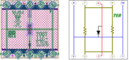
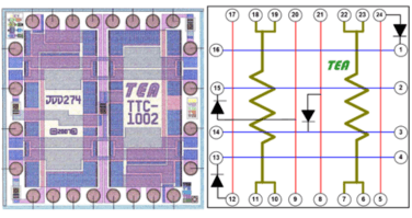
TTCs made from silicon wafers (Figure 1) manufactured in America can accurately simulate the size and non-uniform power distribution (such as hot spots) of a real semiconductor chip, with embedded on-chip sensors for real-time temperature measurement of the chip. The TTC, which is an analog ASIC, is made up of unit cells (Figures 2 & 3), and the power input and temperature ofeachunit cell are directly addressable, thereby providing the capability for configurable power distribution and in situ temperature measurement on the chip – down to the scale of a unit cell.
Metal film resistors are used for the heat source in the unit cell for better uniformity and matching across the wafer, and their relatively stable temperature coefficients result in constant power dissipation over the course of the thermal measurement. The heat sources are also laid out to conform to the JEDEC JESD51-4 standard. Temperature sensing diodes (TSD) strategically located in the TTC allow for precise measurement of the temperature of the die at multiple locations simultaneously.
As the unit cells can be arrayed in any combination, the TTC can be any size to match the size of the real chip (up to 50mm x 50mm or larger if needed). The TTC, with its precision and accuracy of the integrated heaters and sensors in each unit cell can accurately simulate the thermal behavior of a real semiconductor chip and thereby offers a great tool for the concurrent development of thermal management solutions while a new chip is under development (which often takes several years).
Using Thermal Test Chips to Build Test Vehicles
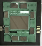
With the TTCs (designed for wire bonding or flip chip attachment), Thermal test vehicles (TTV) can be developed in various packaging formats, such as BGA, LGA, COB, etc., as well as multi-chips per package (Figure 4) to simulate system-in-package (SiP) that is often used in heterogeneous integration.
With the ability for configurable power distribution and simultaneous temperature measurement across the chip, TTCs and TTVs can be very useful for thermal characterization (steady state and transient) and evaluation, including power and/or temperature mapping, for semiconductor packages and devices that can incorporate various thermal management solutions – thermal interface materials (TIM), heat sink, vapor chamber, heat pipe, cold plate, liquid cooling, etc. They can also be very useful for validating thermal simulation and modelling. Furthermore, power cycling can be done in a programmed setting to evaluate the reliability performance of various thermal management solutions.
Thermal Test Chips for Glass Interposers: A Case Study
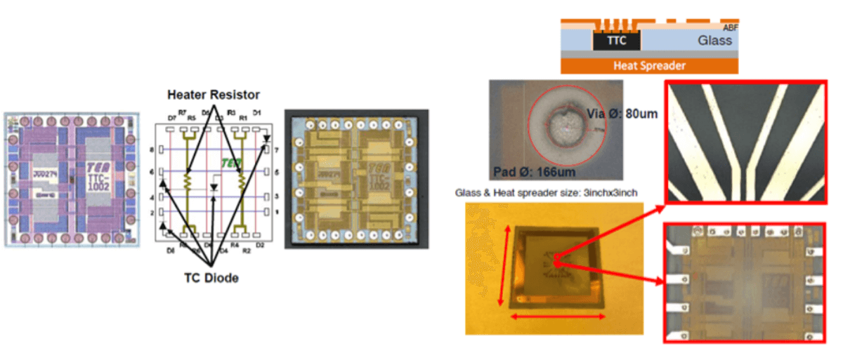
Indeed, TTCs can also meet the needs of advanced packaging. In a recent research project, which was presented at the 2023 IEEE 73rd Electronic Components and Technology Conference (ECTC) in Orlando, FL,in a paperentitled “Bottom Side Cooling for Glass Interposer with Chip Embedding using Double-sided Release Process for 6G Wireless Applications”, researchers from Georgia Tech and Penn State University used TTCs from Thermal Engineering Associates (TEA) for the development of a die-embedded glass interposer process (Figure 5). In the glass interposer, through cavities are prepared in the glass substrate, and the TTC is embedded into the through cavity and connected via redistribution layers (RDL) in the topside. A copper heat spreader is attached to the exposed TTC backside using a TIM interface for thermal management. The embedded TTC power density is tested to see the cooling capacity with various heat transfer coefficients ranging between 28.8~261.3 W/m2K.
Overall, TTCs and TTVs will be able to closely emulate the semiconductor chips and advanced packages as they evolve – with increasing power density and more complex packaging configurations. TTCs in the form of stacked chips and chiplets in 2.5D/3D packaging are currently under development.