
애플리케이션
저온 납땜
저온 납땜은 기술 및 제조 과제의 증가와 지속 가능성에 대한 강조로 인해 인기가 급증하고 있습니다. 업계에서는 다양한 저온 요구 사항에 맞는 합금과 공정을 개발하는 데 점점 더 집중하고 있습니다. 인디엄은 혁신적인 저온 납땜 재료 제품군과 저온 응용 분야에서 수십 년간 쌓아온 전문성을 바탕으로 전자 제품 제조 환경을 변화시키고 있습니다.

개요
지속 가능한 솔루션으로 성능 향상
저온 납땜은 기술적, 환경적 이점을 모두 제공합니다. 열 스트레스를 줄이고, 복잡한 설계를 위한 기술을 발전시키며, 민감한 부품의 뒤틀림이나 손상과 같은 열로 인한 결함을 제거하는 데 도움이 됩니다. 동시에 에너지 비용을 낮추고 탄소 배출량을 줄여 환경 규정을 준수하고 고객의 지속 가능성 목표를 지원합니다.
저온 납땜 애플리케이션
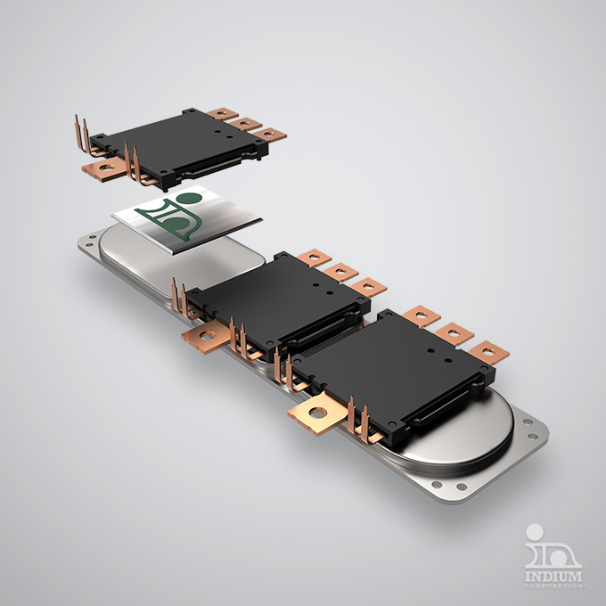
Attachment to Circuit Boards
Attachment of temperature-sensitive components to printed circuit boards.
Step Soldering
Step soldering, when a secondary, lower temperature reflow process is required after a standard SAC soldering process is completed.
Eliminate Warpage
Eliminating warpage of thinner chips due to high-temperature reflow.
IoT Devices
Low melting or low-Tg flex circuitry which are used in cellphones, smartwatches, and many internet-of-things (IoT) devices.
Large Area Array Devices
Large area array devices – such as BGAs – to avoid head-in-pillow (HIP) and non-wet-open (NWO) failures.
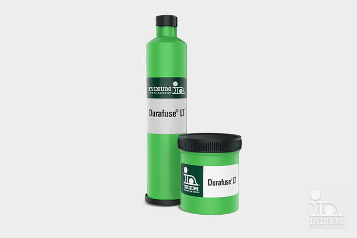
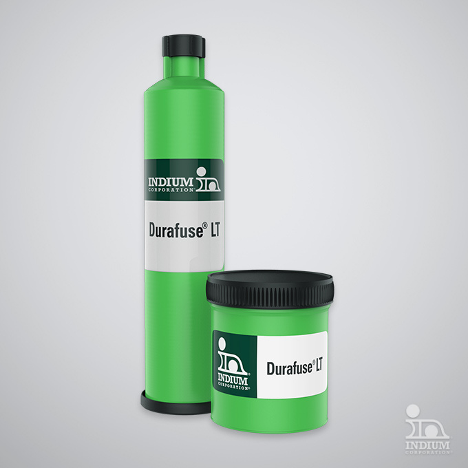
저온 납땜 제품
기존의 인듐 및 비스무트 기반 합금은 물론, 고급 요구 사항을 충족하도록 설계된 혁신적인 Bi+ 및 Durafuse® LT 시리즈를 포함한 다양한 솔더 포트폴리오를 확인해 보세요.
저온 솔더 페이스트
다양한 종류의 저온용 솔더 페이스트.
고신뢰성 페이스트
…용도로 사용되는 다양한 종류의 고신뢰성 솔더 페이스트…
용융성 합금/저융점 합금
Utilize low melting points for easy attachment.
인달로이®301LT
Indalloy® 301LT offers versatile solder forms &…
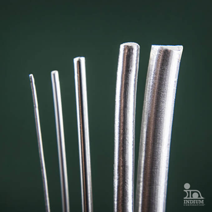
비스무트 와이어
열에 민감한 부품 및 환경 조건에…
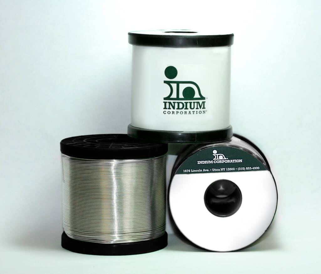
인듐 와이어
인듐 와이어는 낮은 융점, 전도성 등을 갖추고 있으며,…
관련 애플리케이션
밀봉: 극저온 및 완전 밀폐
…용 저온 액체 및 용융 합금
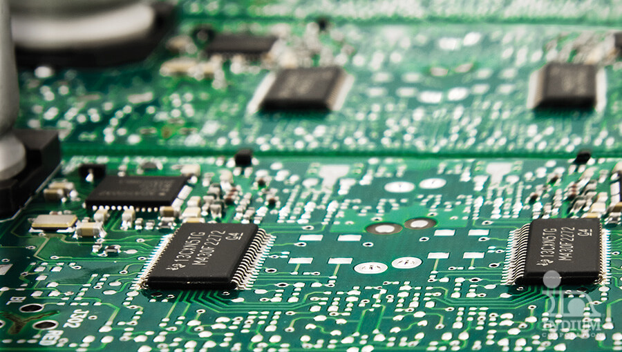
PCB 어셈블리
PCB 조립에 사용되는 검증된 최첨단 소재…
관련 시장
헨켈의 저온 납땜 솔루션은 모바일, 서버, 자동차, 인프라 등 다양한 산업 분야에서 사용됩니다. 당사는 고객과 긴밀히 협력하여 고객의 고유한 애플리케이션에 맞는 맞춤형 솔루션을 제공합니다.


고객의 성공
우리의 목표
최신 재료, 기술 및 전문가 애플리케이션 지원으로 프로세스를 최적화하세요. 이 모든 것은 당사 팀과의 연결에서 시작됩니다.