The next few posts come to us from my colleagues Karthik Vijay, Indium Corporation’s Technical Manager for Europe, and Liam Mills of TT Electronics Power and Hybrid. They’ve done some exciting work using InFORM® technology to make more reliable solder joints at a lower cost than traditional techniques.
– Tim Jensen
As we discussed in Part I of this three-part series, an uneven solder bondline thickness between the substrate and baseplate of an IGBT module can cause stress at the thinner sections1, leading to delamination and premature failure during the operational life of the module. Uniform bondline thickness prevents this stress, though the traditional method of stitching and trimming wirebonds adds time and cost.
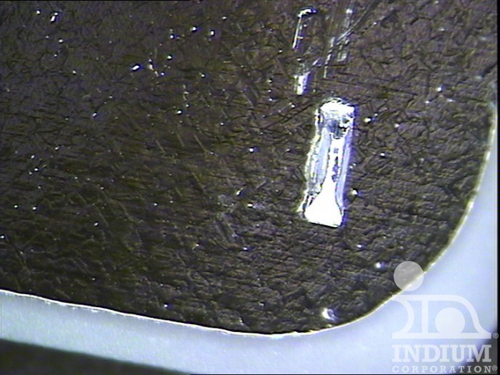
In a quest to find a more efficient means of achieving uniform bondline thickness, TT Electronics Power and Hybrid tested two manufacturing techniques for an aerospace application with thermal cycling reliability specifications of -55/+150°C, 1500 passive cycles. Failure was defined as delamination greater than 50% of substrate/baseplate area and a 200µm-thick desired bondline thickness.
The first technique included the use of solder preforms followed by trimmed wirebonds. In this study, wirebonds were stitched and trimmed to the required bondline of 200µm at the corners of the substrate/baseplate. An Sn63/Pb37 solder preform was then placed and soldered to the substrate and baseplate. The modules passed the 1500 passive thermal cycles spec with no delamination. Voiding was within the acceptable limits of less than 5% due to optimized process conditions.
This is a perfectly valid method of achieving a reliable end product; however, we still suffer from the disadvantage of extra steps and the costs associated with such actions.
Check back for the final part of this series when we explore the results of using InFORMS® to achieve uniform bondline thickness.
Best,
Karthik Vijay, Indium Corporation, UK, kvijay@indium.com and
Liam Mills, TT Electronics Power and Hybrid, UK, liam.mills@semelab-tt.com
References
- K. Hayashi & G. Izuta, “Improvement of Fatigue Life of Solder Joints by Thickness Control of Solder with Wire Bump Technique,” ECTC 2002, www.cpmt.org/proceedings/