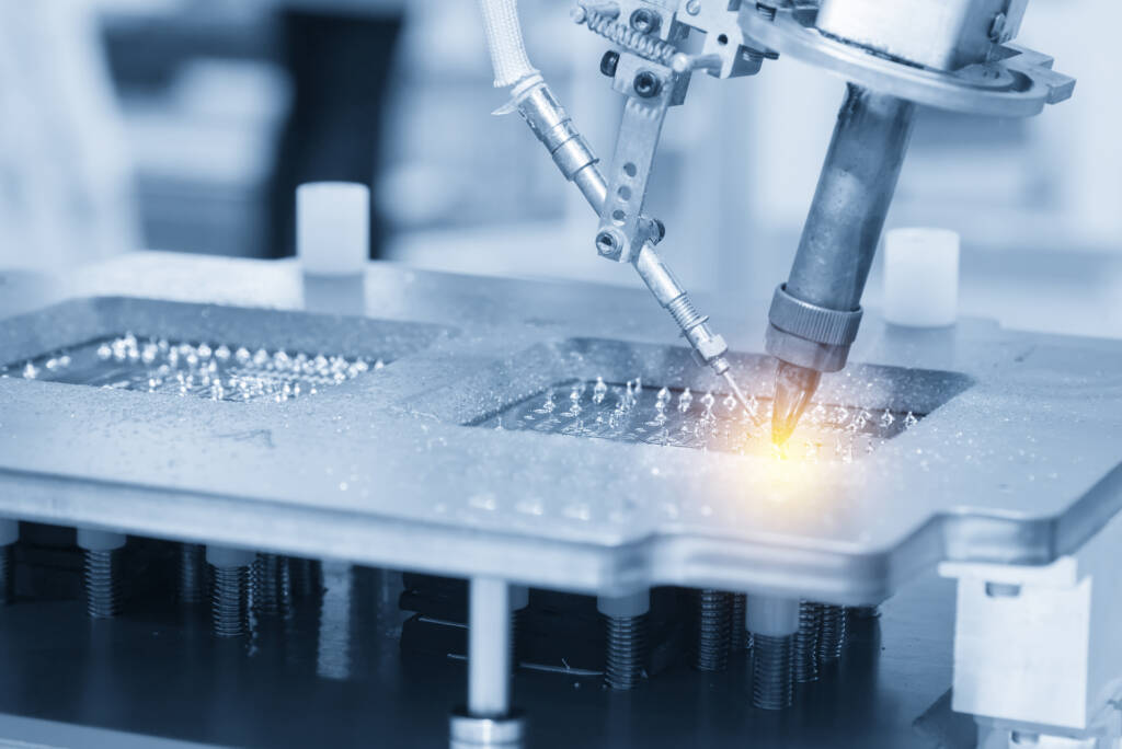
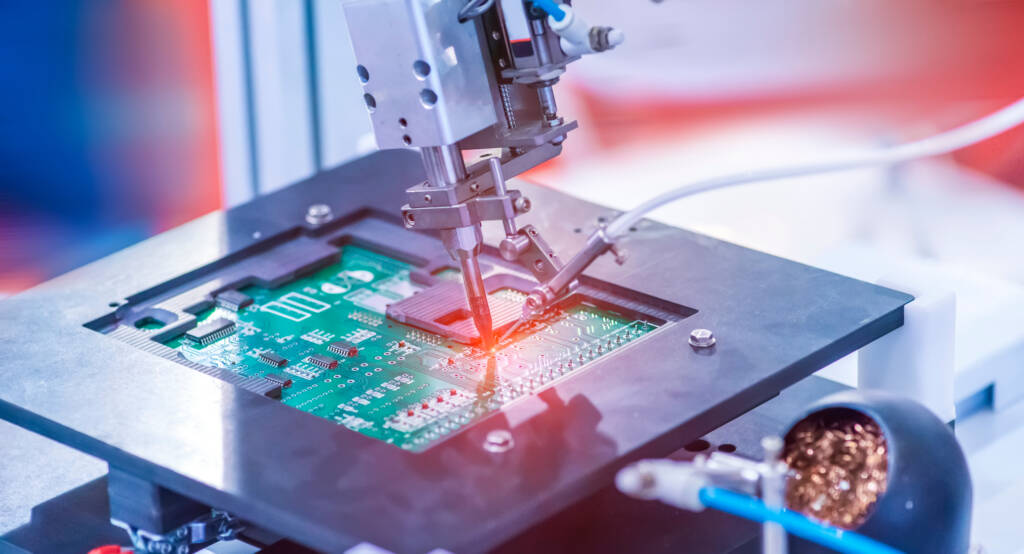
I was asked this week to contribute to the upcoming IPC handbook (IPC-CH-65 HDBK) on the section on contamination and its effects on printed wiring assemblies (PWA’s). There is a clear crossover of technology from the standard SMT / PCB arena into semiconductor assembly: specifically into flip-chip, microbumps and TSV assembly. However, the terminology is “starting to collide”: phrases familiar to semiconductor manufacturers now need to be understood and become part of the lexicon of semiconductor packaging engineers coming into the field from SMT. I want to set the record straight about this, hence this blog posting, which is based on a paper I gave at the IWLPC meeting in 2009, but probably bears repeating for a wider audience.
电化学迁移(ECM)
ECM is characterized by the movement of metal ions BETWEEN adjacent metal conductors, to form dendrites. The key control parameters here are:
-湿度或高湿度,以 %RH 度量
–Presence of mobile metal ions
-高电位梯度,以每单位长度伏特(V/cm)表示
High temperature may also exacerbate the problem. The hydrated metal ions, being positively charged, will migrate towards the cathode (-ve), forming a dendrite, which is a needle or tree-branch-like metal structure. The dendrite is the primary visual indicator of ECM. 
Electromigration (EM)
另一方面,电磁发生在金属导体内部,当大量高速电子撞击金属原子并通过简单的动量传递使其移位时,就会产生电磁。影响电磁的主要因素有
-高温
–Presence of mobile metal atoms
–A high current density, expressed in Amps per unit area (say A/cm2)
值得注意的是,湿度或其他环境湿度对电磁没有影响,因为电磁发生在金属接头内部。

The primary visual indicator of EM is the presence of voids at points in a metal interconnect near the anode (+ve), often where the current density is greatest (the “current crowding” effect – see below). 
The voids are usually seen inside the joint, and can eventually lead to thermal runaway and joint failure, as the effective cross-sectional area of the joint shrinks over time, increasing the current density.
希望我的解释清楚、合理。
干杯安迪