有时,我会收到这样的问题:"使用你们的氨基磺酸铟浴,在我的平板上沉积 20 µmof 的铟需要多长时间?要回答这个问题,对客户来说非常容易。在本篇文章中,我将为大家介绍一个简单易行的关系式。相信我,这很简单;只需使用我们在高中学习过的一些基本关系。首先要知道将一个In3+离子还原成一个In原子需要多少个电子--3,没错!
那么,收费是多少 - 3e!
所需的时间直接取决于我们需要提供多少电荷来还原所有这些铟离子,以及我们能以多快的速度提供这些电荷--这就是 "电流"!
如果您听说过这一著名的电流-电荷关系、 是的,我说的就是这个意思。
所以,还是回到最基本的话题吧、


如果阴极(电沉积铟的地方)不是 效率越高,所需的时间就越长。假设 σ 是效率。那么需要 倍。例如 高效,这需要时间、 倍。因此,考虑到效率,时间等式变为:
将所有这些值输入上面的等式,就得到了:
好的,那么答案就是,预计存款时间 是 34 分钟,你知道有哪些因素可以改变这个时间。
And here’s an easy formula to calculate time in minutes for the most widely used units of thickness and current density;
好吧,为什么不打这个电话呢? "Shital的Inplate常数"!![]()
Indium Sulfamate Bath from Indium Corporation has a cathodic efficiency of 90%. More efficiency means less time! The typical current density to work on is around 但可以增加到 将水浴温度保持在 . Increasing the current density from 至 可将沉积时间缩短 5 倍,即相同的 现在将在 7 分钟内存入。
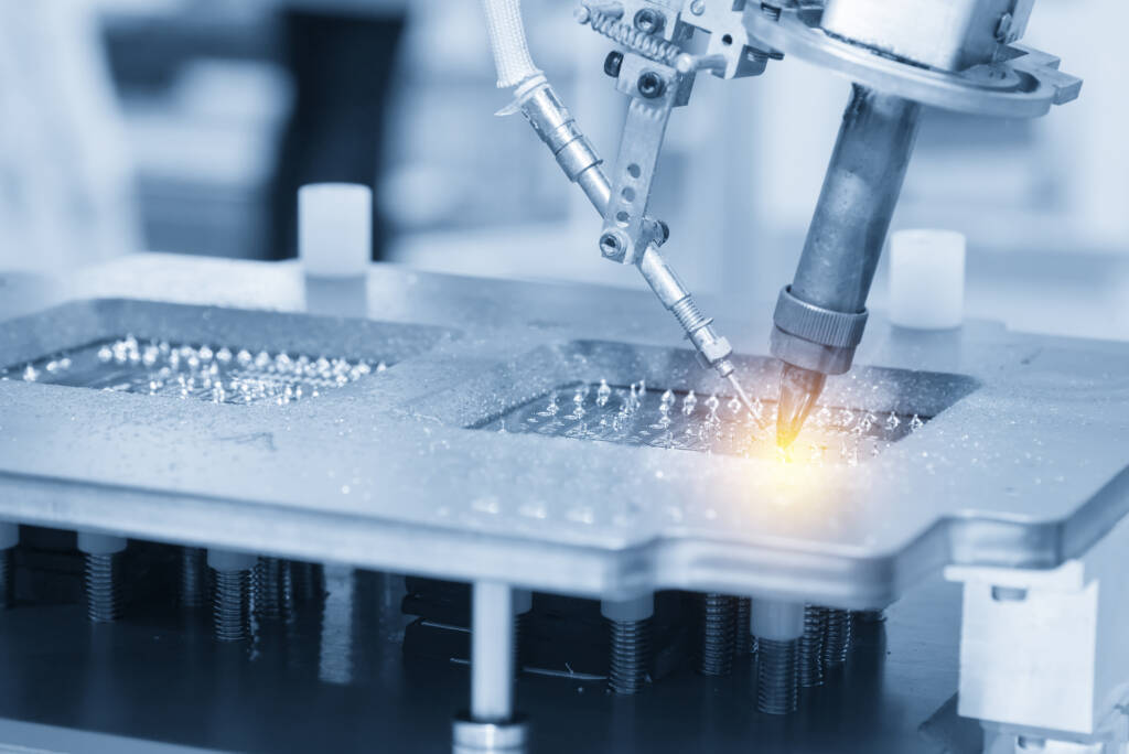
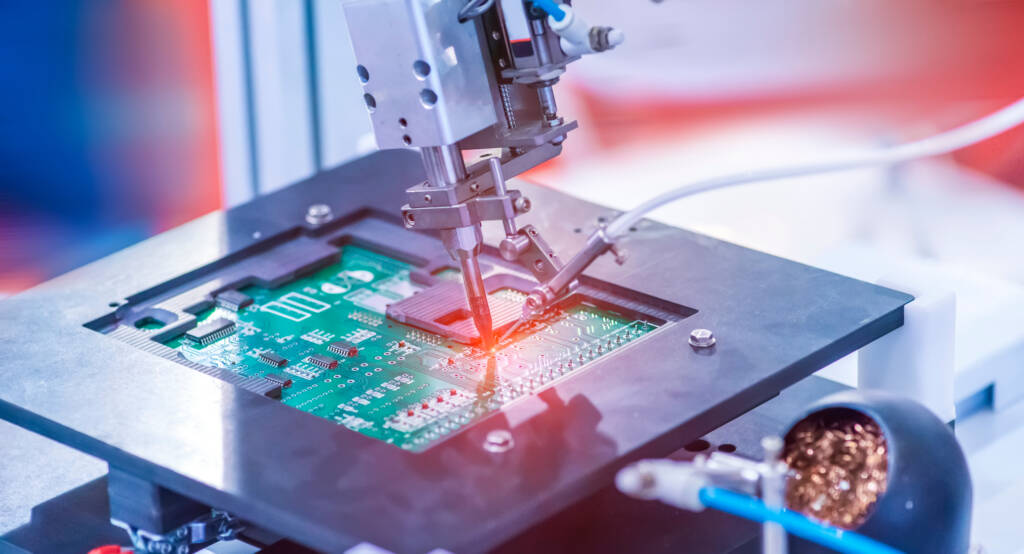
The extensive use of indium plating today dates back to the 1930s when the founders of Indium Corporation developed a commercial indium plating bath for the first time. Recent developments in semiconductor technology and flip-chip bonding utilize indium to create interconnects between layers of wafers. Indium is electroplated onto wafer substrates to create high-density, low-pitch and high-aspect ratio indium bumps. The softness, ductility and wettability of Indium ensure a strong and reliable connection between two surfaces, even if they are not perfectly flat or aligned. Furthermore, Indium exhibits stability even at temperatures approaching zero, making it highly suitable for use in semiconductor applications that operate in extreme environments, such as those encountered in space.
如果您想进行小规模电镀项目,包括用铟镀层修复古董金属物品,您可以从这里提供的这种健康易用的电镀套件开始。
Please refer to the following documents to learn more about indium electroplating, Indium Sulfamate Bath, and indium bump electroplating.
- Achieving a Finer Grain Structure Using the Indium Sulfamate Plating Bath
- Indium Bump Electroplating of Wafers Using Pulse Plating
- 电镀,涂铟的另一种方法
- 镀铟的正确表面处理方法
- Prototype Plating Using Indium Sulfamate Plating Bath
- Reclamation & Disposal of Indium Sulfamate Plating Bath Solution
如有任何疑问,请与我联系。![]()