這篇關於利用超細焊錫膏進行表面貼裝技術(SMT)優化中「網版印刷」環節的系列文章最終篇,將我們先前討論的所有內容彙整起來,並探討焊錫顆粒大小所產生的影響。 以下部分資訊是我於 2014 年 5 月在多倫多 SMTAI 會議上所發表的內容。這些發現是基於一項焊錫膏印刷實驗,該實驗旨在區分不同類型焊錫粉之間的轉移效率與 一致性。為了減少變因數量,實驗中採用了相同的網版、刮刀片及印刷機參數。
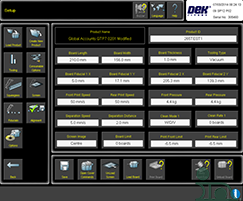
圖 1. 實驗用 印表機設定
實驗中使用了厚度為 4 mil 的雷射切割網版、配備邊緣護板的 250 mm 刮刀、無箔夾具,以及橫向真空支撐塊。 圖 1 顯示了實驗中使用的印刷機設定。每種焊錫膏均以 50 mm/s 的速度進行印刷,刮刀壓力為 4.4 kg,分離速度為 5 mm/s,分離距離為 2 mm。僅在為期 1 小時的「濕/乾/真空」(W/D/V)暫停期間,才採用底部網版擦拭法。
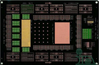
圖 2. 測試 車輛
選定了一台測試機台(圖 2),重點針對 6、7、8、9、10 及 12 mil 的圓形與方形元件,以及 0201 焊盤(包含由阻焊層界定的 SMD 焊盤與非阻焊層界定的 NSMD 焊盤)。 評估了四種粉末類型(3、4、5 及 6),分別應用於免清洗型與水溶性助焊劑配方中。透過連續印刷 20 次、暫停 1 小時,再印刷 6 次的方式,測量其「暫停後響應」表現。 在印刷前 20 片印刷電路板後,立即進行 W/D/V 模板擦拭。採用Koh Young KY-3020T 雷射掃描系統測量模板印刷沉積物的體積,共收集 1,386,500 個數據點(焊膏沉積點)。
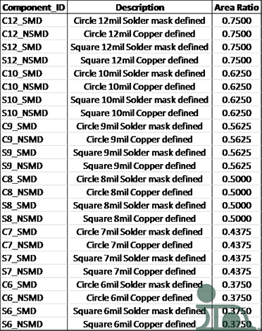
圖 3.焊盤標籤、說明及相關面積比
圖 3 顯示了元件的識別資訊及其對應的面積比。
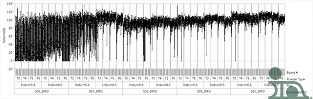
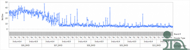
圖 4. 測試結果的整體概覽
Figure 4 represents a broad view of the resultant test data. The y-axis of the upper graph indicates the transfer efficiency in volume %. The bottom graph indicates the standard deviation of the process: <10% standard deviation and 100% transfer efficiency is our goal.
在我們的調查過程中,我們剔除了 0201 及 12mil 晶片級封裝 (CSP) 測試焊盤的測試數據:這些數據未顯示於圖 4 中。無論使用何種粉末或助焊劑類型,這些焊盤上的焊膏沉積均印刷良好,因此未納入後續調查範圍。圖 4 中的數據顯示,最小的測試開口(6mil)在所有粉末類型或助焊劑載體下均未能良好印刷。 6mil 開口的面積比相當小(0.375),而測試結果至少可說是參差不齊。
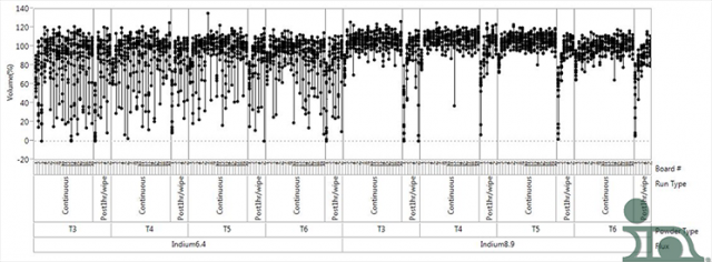
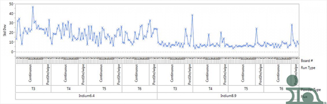
圖 5. 定義為 7mil 正方形阻焊層的焊盤結果範例
Figure 4 revealed a dramatic improvement with 7mil apertures that deserved further investigation, notably between the water-soluble and no-clean flux formulations. Figure 5 shows the improvement in more detail by expanding the view of the 7mil aperture and breaking out the data before and after the 1-hour pause. The comparison is very typical when comparing no-clean and water-soluble solder pastes. Note that a standard deviation of <10%, with the exception of a few outliers was evidenced, specifically with the no-clean flux chemistry (Indium8.9). The area ratio for the 7mil aperture is 0.4375. The transfer efficiency was near the target (100%) and improved as the powder type moved toward type 6. Type 5 exhibited the best results—a narrow distribution in volume percent and low standard deviation except after first pause. It is important to note that the significant drop in transfer efficiency after the 1-hour pause was not consistent with previous experiments. For all solder pastes tested, this was attributed to a very low humidity (<10%) and had a dramatic effect on the first print after sitting on the stencil for 1 hour.
在實驗中,透過運用前幾篇文章所涵蓋的所有優化流程/準則,所達成的最佳面積比為 0.4375。較細的粉末,結合阻焊層定義的焊盤、具有圓角的方形開孔絲網版,以及免清洗助焊劑配方,成功提升了面積比。