Included in a solder paste’s Product Data Sheet, among other things, are general guidelines which aid the customer in designing an SMT reflow profile. The data sheet gives general recommendations, for time above liquidus, peak temperature, and ramp rate.
例:
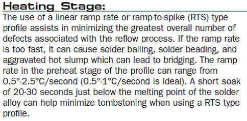
Figure 1: Example shown Indium8.9 flux with SAC lead-free alloy
この主題を取り上げる理由は、最大勾配(ほとんどのプロファイリングソフトウェアで報告されるカテゴリ)とデータシートに記載されているランプ率の違いに関して、しばしば混乱が生じてきたためである。
最大傾斜は、PCBが周囲温度からオーブン内に移動する最初のゾーンで達成されることが非常に多い。ほとんどの場合、最初のゾーンのオーブンゾーン設定は100℃以上です。この場合、周囲温度と最初のゾーン間の温度変化は最低75℃(周囲温度を25℃と仮定)であるため、ほとんどの場合、最大の温度変化(最大勾配)は最初のゾーンにあることがわかります。
最大勾配の焦点は、熱衝撃を避けるため、コンポーネントの観点から、通常3℃/秒が上限として推奨される。
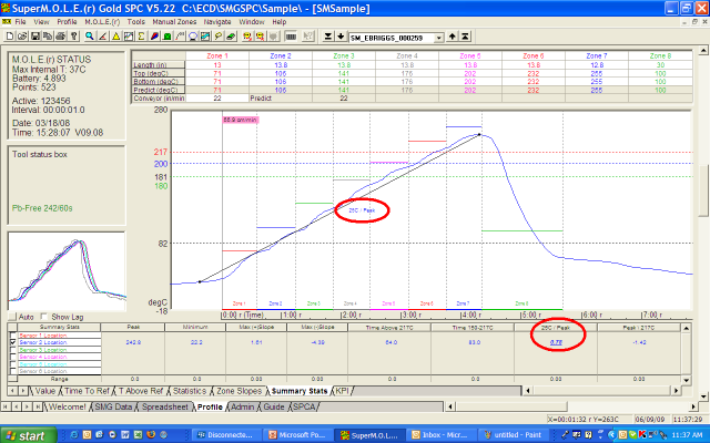
Figure 2. Ramp or Average Rate
ランプレートは、周囲温度(室温)からピーク温度までの変化率(時間当たりの温度変化)としてより適切に説明できる。また、ランプからスパイクへのプロファイルにおいてより実用的に用いられる。
From the view point of the solder paste, the lower the ramp rate the better, usually 1-2°C/s. This is to drive off volatiles and help minimize solder defects such as solder balling, solder beading, and tombstoning. This rate becomes even more important as the solder paste deposit continually decreases in size, as we move to 0201’s and smaller discrete components and from 0.5mm pitch area array packages to 0.4mm and smaller. Due to this miniaturization, the observance of graping and head-in-pillow have become more common. The reflow process window is becoming very narrow and this attribute (ramp rate) has become as important as time above liquidus and peak temperature.
この件が貴社のSMTプロセスに影響を与えている場合、ぜひご一緒に議論させていただきたいです。お気軽に私までご連絡ください。